Liquid crystal display panel, liquid crystal waveguide display device and manufacturing method of liquid crystal display panel

A technology for a liquid crystal display panel and a manufacturing method, which is applied to instruments, nonlinear optics, optics, etc., can solve the problems of poor uniformity, less light total, low contrast, etc., so as to improve the overall structural strength, reduce the manufacturing cost, and improve the transition sexual effect

Active Publication Date: 2020-08-04
BOE TECH GRP CO LTD
View PDF4 Cites 0 Cited by
  • Summary
  • Abstract
  • Description
  • Claims
  • Application Information

AI Technical Summary

Problems solved by technology

[0005] However, when the liquid crystal waveguide display device in the prior art is displayed, there are still less luminous fluxes in the liquid crystal layer, so that when the liquid crystal molecules scatter light to the incident light, the available The total amount of light

Method used


Image

  • Liquid crystal display panel, liquid crystal waveguide display device and manufacturing method of liquid crystal display panel
  • Liquid crystal display panel, liquid crystal waveguide display device and manufacturing method of liquid crystal display panel
  • Liquid crystal display panel, liquid crystal waveguide display device and manufacturing method of liquid crystal display panel

Examples


Example Embodiment

[0046] In order to explain the present invention more clearly, the present invention will be further described below in conjunction with preferred embodiments and drawings. Similar components in the drawings are denoted by the same reference numerals. Those skilled in the art should understand that the content described below is illustrative rather than restrictive, and should not be used to limit the protection scope of the present invention.
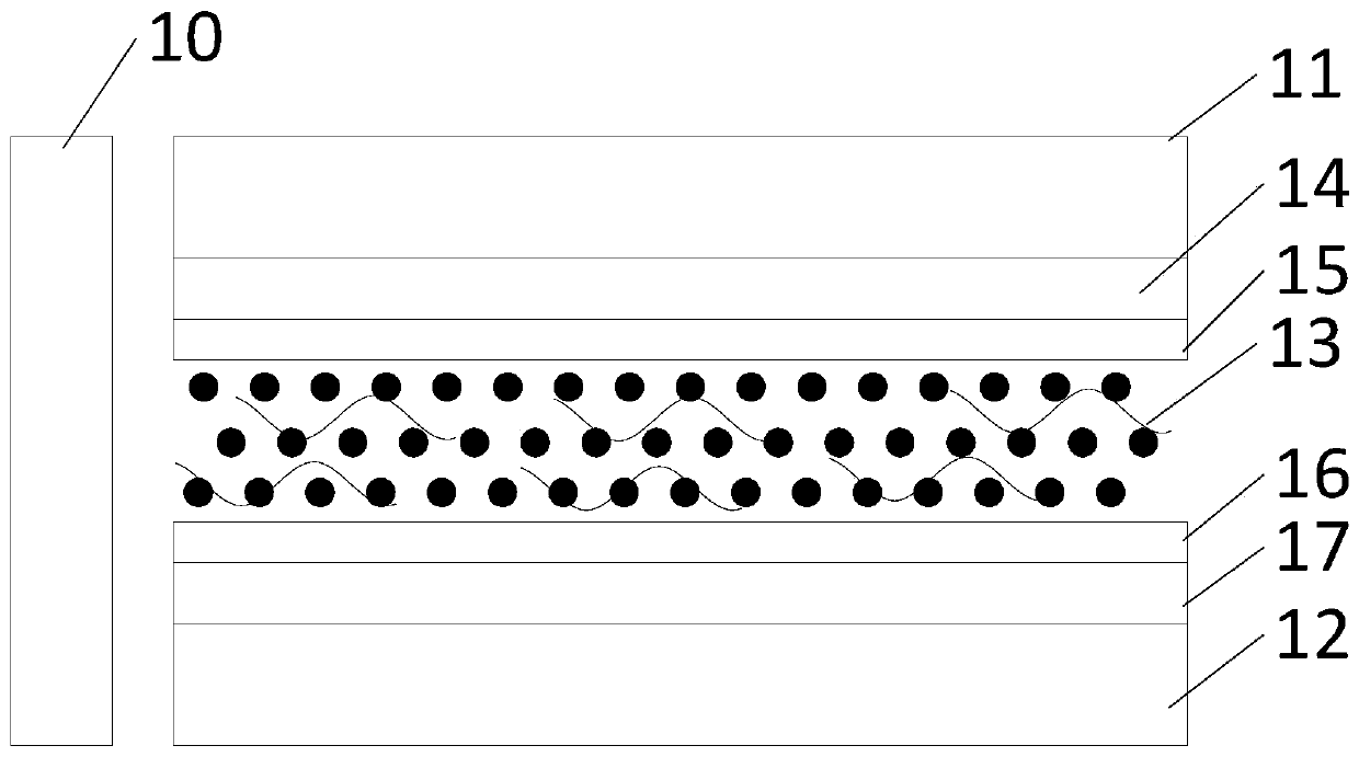
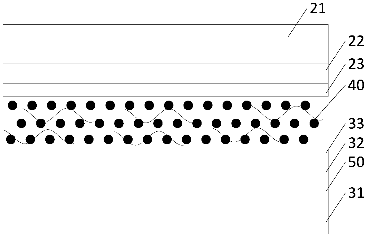
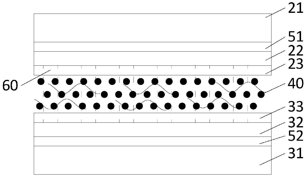
[0047] In view of the technical problems existing in the prior art, the present invention provides a liquid crystal display panel, such as Figure 2-3 As shown, the liquid crystal display panel includes a first substrate and a second substrate disposed opposite to each other, and a liquid crystal layer 40 located between the first substrate and the second substrate. The first substrate includes a first transparent substrate 21 and The first transparent electrode layer 22 is formed on the side of the first transparent substrate 21 close to...


PUM

PropertyMeasurementUnit
Thicknessaaaaaaaaaa
Thicknessaaaaaaaaaa

Abstract

The invention discloses a liquid crystal display panel, a liquid crystal waveguide display device and a manufacturing method of the liquid crystal display panel. A first base plate, a second base plate and a liquid crystal layer are included, wherein the first base plate and the second base plate are oppositely arranged, and the liquid crystal layer is located between the first base plate and thesecond base plate. The first base plate comprises a first transparent substrate and a first transparent electrode layer formed on one side, close to the liquid crystal layer, of the first transparentsubstrate; the second base plate comprises a second transparent substrate and a second transparent electrode layer formed on one side, close to the liquid crystal layer, of the second transparent substrate; and at least one of the first base plate and the second base plate comprises a refractive index transition layer, the refractive index transition layer is formed between the corresponding transparent substrate and the transparent electrode layer, and the refractive index of the refractive index transition layer is between the refractive index of the corresponding transparent substrate and the refractive index of the transparent electrode layer. By arranging the refractive index transition layer, the refractive indexes of the corresponding transparent substrate and the transparent electrode layer are better matched, an available luminous flux in the liquid crystal display panel is improved, and utilization efficiency of a light source is increased.

Description

technical field [0001] The invention relates to the technical field of transparent display, in particular to a liquid crystal display panel, a liquid crystal waveguide display device and a manufacturing method of the liquid crystal display panel. Background technique [0002] With the increasing development of display technology, various new technologies are constantly emerging. Among them, transparent display technology has gradually entered people's lives. Transparent display devices generally refer to the ability to form a transparent display state so that viewers can see the display in the display device. Display devices for images and scenes behind display devices, such as transparent windows, vending machines, transparent wearables, smart homes, etc. Transparent display technology has broad application prospects. [0003] The light transmittance of a common traditional liquid crystal transparent display device in the prior art is generally lower than 20%, and requires ...

Claims


Application Information

Patent Timeline
IPC IPC(8): G02F1/1335G02F1/137
CPCG02F1/133502G02F1/137G02F1/13775
Inventor 王龙彭依丹贾南方
Owner BOE TECH GRP CO LTD
Why Eureka
Try Eureka