Semiconductor memory device

A memory and semiconductor technology, applied in semiconductor devices, static memory, digital memory information, etc., can solve the problem of increased power consumption, and achieve the effect of reducing the maximum power consumption and reducing the average power consumption

Inactive Publication Date: 2003-07-16
PS4 LUXCO SARL
View PDF4 Cites 0 Cited by
  • Summary
  • Abstract
  • Description
  • Claims
  • Application Information

AI Technical Summary

Problems solved by technology

Therefore, the problem of increased power consumption caused by charging and discharging of the write bus can no longer be ignored

Method used


Image

  • Semiconductor memory device
  • Semiconductor memory device
  • Semiconductor memory device

Examples


Embodiment Construction

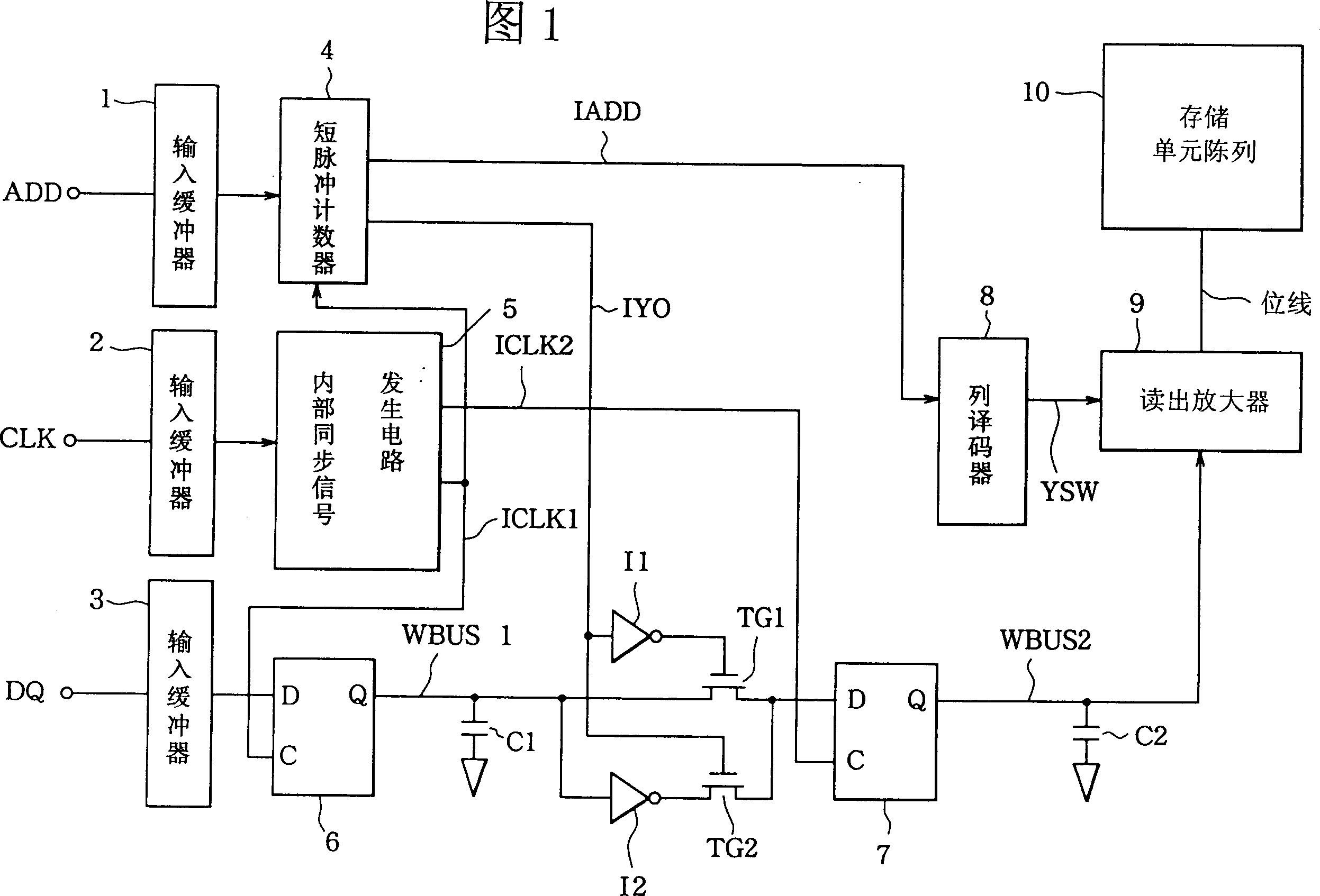
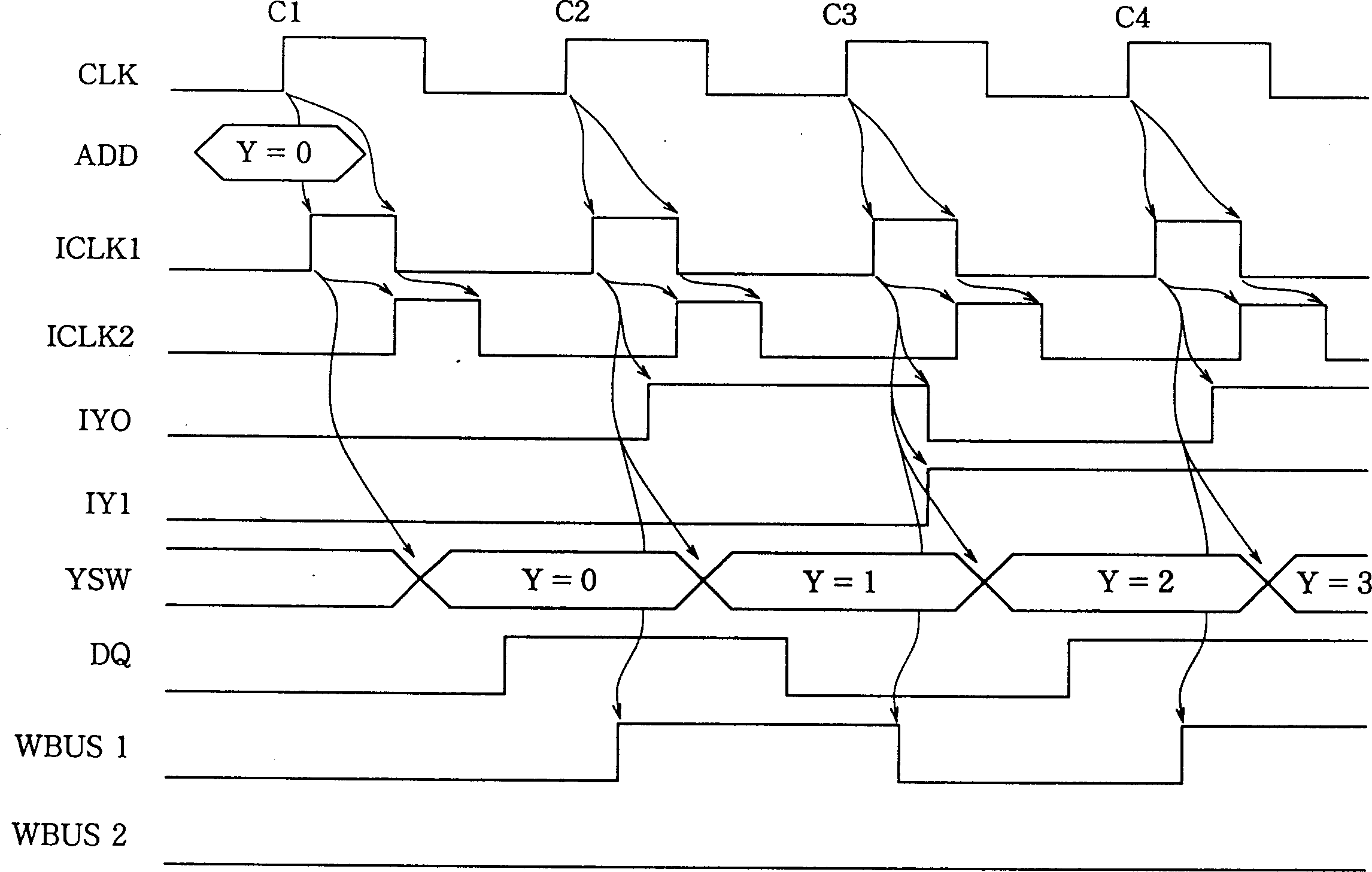
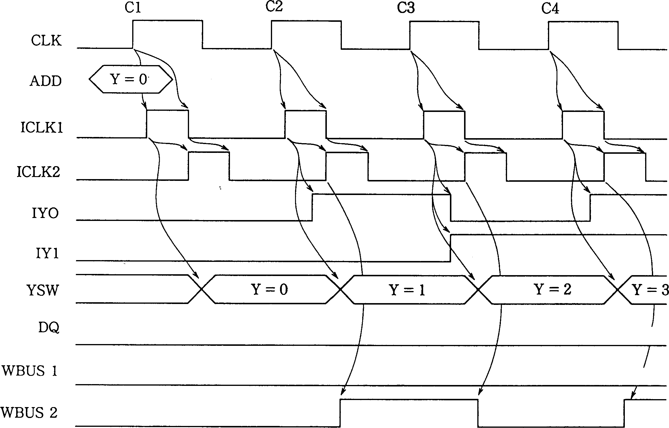
[0034] Preferred embodiments of the present invention will be described below in conjunction with the accompanying drawings. FIG. 1 is a schematic diagram showing the circuit structure of the first embodiment of the present invention. An example of the invention applied to a write data bus is shown. According to its preferred embodiment, the semiconductor memory of the present invention includes: an internal synchronous signal generating circuit 5 (Fig. 1), which is used to generate internal synchronous signals ICLK1, ICLK2 ( figure 2 ); short pulse counter 4 (Fig. 1), utilizes the external address input from the outside during the first period of said reference signal as a starting address, and forms an internal address signal (IADD) in a certain order synchronously with an internal synchronous signal; The data bus is used to transmit the storage data of the storage unit; and according to the lowest bit address (IY0 ) level, the circuit device that inverts the polarity of t...


PUM


Abstract

An internal synchronous signal generating circuit outputs the internal synchronous signals ICLK1, ICLK2. A burst counter outputs an internal column address signal IADD and the lowermost internal column address signal IY0. A D-F/F input an output of the input buffer and drives a write bus (WBUS1) in synchronization with the ICLK1. An inverting element inputs IY0. Inverting elements input outputs of the D-F/F6 and D-F/F7 and drives a write bus (WBUS2). A column decoder inputs IADD and outputs a column switch YSW. Sense amplifiers input the YSW and the second WBUS. By this device, the maximum consumptive current amount or an average consumptive current in the burst can be reduced.

Description

technical field [0001] The present invention relates to a semiconductor memory, and more particularly to a data path control circuit designed to reduce the charging and discharging current of the data path. Background technique [0002] In recent years, as the speed of CPUs has increased, the demand for high operating speeds of semiconductor memories has increased. To meet these needs, synchronous type semiconductor memories have been proposed, which operate synchronously with an external clock exceeding 100 MHz. Existing documents on such semiconductor memories include, for example, Japanese Patent Application Laid-Open No. 61-148692 (Title of Invention: Memory), Japanese Patent Application Laid-Open No. 6-76566 (Title of Invention: Semiconductor Memory), Japanese Patent Application Laid-Open No. 7- 45068 (name of invention: synchronous semiconductor memory) and the like. [0003] An example of the structure of these conventional synchronous type semiconductor devices is ...

Claims


Application Information

Patent Timeline
Patent Type & Authority Patents(China)
IPC IPC(8): G11C11/41G11C7/10G11C7/22G11C8/18G11C11/407G11C11/409H01L27/10
CPCG11C7/1048G11C8/18G11C7/1018G11C7/22G11C11/407
Inventor 越川康二
Owner PS4 LUXCO SARL
Why Eureka
Try Eureka