Fingerprint chip module preparation method, fingerprint chip module and electronic device

A fingerprint chip and module technology, applied in circuits, electrical components, electrical solid-state devices, etc., can solve the problems of complex structural design of finished products, increased cost and production difficulty, and reduced product yield, etc., to achieve simple structure and improved yield. , the effect of increasing the conductive area

Active Publication Date: 2020-08-18
SHENZHEN CHIPSBANK TECH
View PDF5 Cites 0 Cited by
  • Summary
  • Abstract
  • Description
  • Claims
  • Application Information

AI Technical Summary

Problems solved by technology

The standby power consumption of this solution is 6-10uA, and a metal ring must be added around the fingerprint sensor, which will greatl

Method used


Image

  • Fingerprint chip module preparation method, fingerprint chip module and electronic device
  • Fingerprint chip module preparation method, fingerprint chip module and electronic device
  • Fingerprint chip module preparation method, fingerprint chip module and electronic device

Examples


Example Embodiment

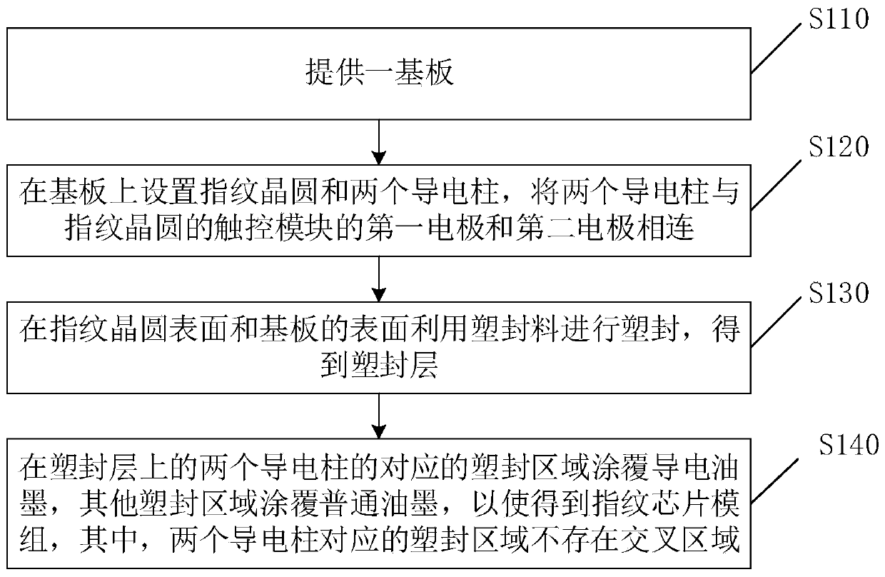
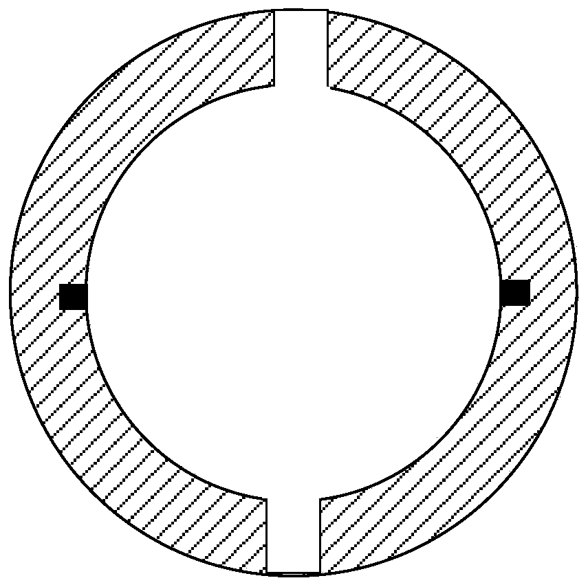
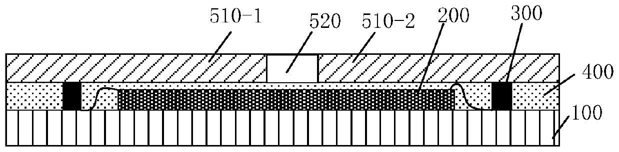
[0039] At present, in related technologies, a touch key is connected to a metal ring to realize standby wake-up and reduce standby power consumption of the fingerprint chip. After the fingerprint chip enters sleep mode, the system automatically cuts off the power of the fingerprint sensor and MCU, leaving the Touch key on standby to wake up the MCU and fingerprint sensor after a finger touch. The standby power consumption of this solution is 6-10uA, and a metal ring must be added around the fingerprint sensor, which will greatly increase the cost and production difficulty, complicate the finished product structure design, and reduce the yield rate of the product. Based on the above technical problems, this embodiment provides a method for preparing a fingerprint chip module. The traditional outer metal ring is replaced by conductive pillars and coated with conductive ink on the corresponding area of ​​the fingerprint chip, and the conductive ink is used to increase the conducti...


PUM


Abstract

The invention provides a fingerprint chip module preparation method. The method comprises the following steps of providing a substrate; arranging a fingerprint wafer and two conductive columns on thesubstrate, and connecting the two conductive columns with a first electrode and a second electrode of a touch module of the fingerprint wafer; carrying out plastic package on the surface of the fingerprint wafer and the surface of the substrate by using a plastic package material to obtain a plastic package layer; and coating the corresponding plastic package areas of the two conductive columns onthe plastic package layer with conductive ink, and coating the other plastic package areas with common ink, so that the fingerprint chip module is obtained, wherein the plastic package areas corresponding to the two conductive columns do not have an intersection area. According to the present invention, the conductive columns and the corresponding areas of the fingerprint chip are coated with thecoating, namely the conductive ink, a traditional external metal ring is replaced, the conductive area is increased through the conductive ink, a metal ring used for standby awakening of the touch key chip is omitted, the structure is simple, and then the yield of products is increased. The invention further provides a fingerprint chip module and an electronic device which both have the above beneficial effects.

Description

technical field [0001] The present application relates to the field of semiconductor technology, in particular to a method for preparing a fingerprint chip module, a fingerprint chip module and electronic equipment. Background technique [0002] At present, in related technologies, a touch key is connected to a metal ring to realize standby wake-up and reduce standby power consumption of the fingerprint chip. After the fingerprint chip enters sleep mode, the system automatically cuts off the power of the fingerprint sensor and MCU, leaving the Touch key on standby to wake up the MCU and fingerprint sensor after a finger touch. The standby power consumption of this solution is 6-10uA, and a metal ring must be added around the fingerprint sensor, which will greatly increase the cost and production difficulty, complicate the finished product structure design, and reduce the yield rate of the product. [0003] Therefore, how to provide a solution to the above technical problems...

Claims


Application Information

Patent Timeline
IPC IPC(8): H01L21/56H01L23/00H01L23/31H01L23/498G06K9/00
CPCH01L21/56H01L24/85H01L23/49811H01L23/3121G06V40/13Y02D10/00
Inventor 张华龙李华伟罗小林
Owner SHENZHEN CHIPSBANK TECH
Why Eureka
Try Eureka