Packaging conductive structure and method for manufacturing the same

a technology of conductive structure and packaging, which is applied in the direction of semiconductor devices, electrical equipment, semiconductor/solid-state device details, etc., can solve the problems of limited structure and material, breakage, and inapplicability of conventional wire bonding techniques for connecting semiconductor chips to other devices, so as to enhance the capability of junction buffer, reduce the possibility of breakage, and increase the contact area

Active Publication Date: 2011-03-29
CHIPMOS TECH INC
View PDF10 Cites 7 Cited by
  • Summary
  • Abstract
  • Description
  • Claims
  • Application Information

AI Technical Summary

Benefits of technology

[0011]The primary objective of this invention is to provide a packaging conductive structure for a semiconductor substrate and a method of manufacturing the same. At least one auxiliary component is disposed in the packaging conductive structure to increase the contact area between the bump conductive layer and bump. This auxiliary component may also provide an elastic buffer to further enhance the capability of junction buffer and lower the possibility of breakage between the bump and bump conductive layer.
[0012]Another objective of this invention is to provide a packaging conductive structure for a semiconductor substrate and a method of manufacturing the same. The conductive area may be increased with rearrangement of the UBM and bump conductive layer, enhancing the capability of the junction buffer and further improving the conductivity thereof.

Problems solved by technology

Due to the miniaturization, the conventional wire bonding techniques for connecting semiconductor chips to other devices are no longer applicable.
However, in the conventional packaging conductive structure, the capability of the junction buffer of the bump 19 on the UBM 17 is limited in structure and material.
Once the process proceeds with poor control or improper selections of the materials, a breakage may occur due to the poor junction in the bump 19.
As a result, the bump 19 may peel off and cause the semiconductor chip to fail.

Method used


Image

  • Packaging conductive structure and method for manufacturing the same
  • Packaging conductive structure and method for manufacturing the same
  • Packaging conductive structure and method for manufacturing the same

Examples


Embodiment Construction

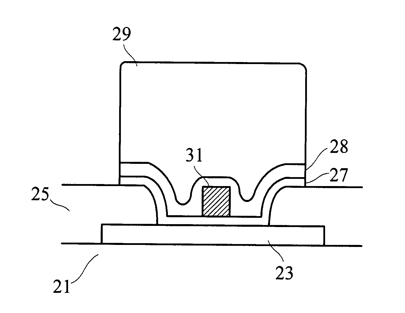
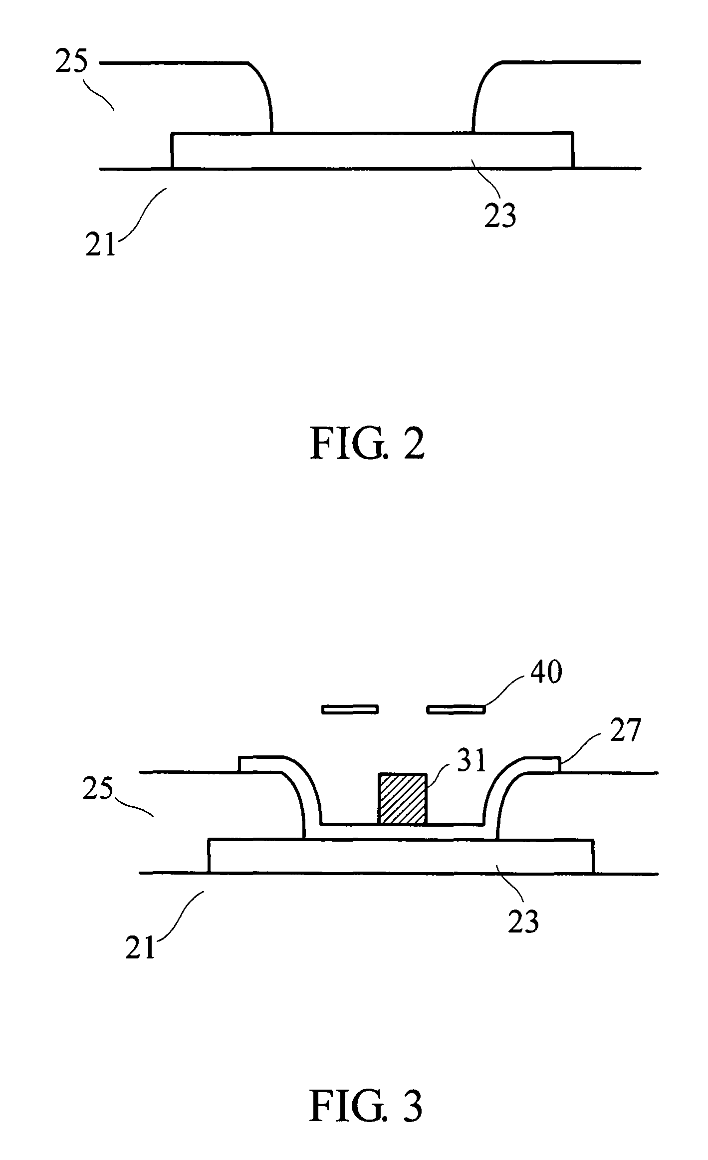
[0021]A packaging conductive structure for a semiconductor substrate and a method of manufacturing the same are disclosed in the present invention. First, in reference to FIG. 2, a semiconductor substrate 21 comprises a pad 23 disposed thereon. The pad 23 is usually made of aluminum and serves as a contact point between the semiconductor structure within the semiconductor substrate 21 and external devices. Then, a passivation layer 25 is formed on the semiconductor substrate 21 for partially overlaying the pad 23 and defining a receiving space. During the manufacturing process, a photoresistance layer may be previously formed for the etching process to remove the unnecessary portions of the photoresistance material after patterning. The receiving space is then formed with a portion of the pad 23 exposed.

[0022]In FIG. 3, an under bump metal (UBM) 27 is formed in the receiving space for an electrically connection to the pad 23 of the semiconductor substrate 21, wherein the UBM 27 is m...


PUM


Abstract

A packaging conductive structure for a semiconductor substrate and a method for manufacturing the structure are provided. The structure comprises an under bump metal (UBM) that overlays a pad of the semiconductor substrate. At least one auxiliary component is disposed on the UBM. Then, a bump conductive layer is disposed thereon and a bump is subsequently formed on the bump conductive layer. Thus, the bump can electrically connect to the pad of the semiconductor substrate through the UBM and the bump conductive layer and can provide better junction buffer capabilities and conductivity.

Description

[0001]This application claims benefits from the priority of Taiwan Patent Application No. 096106253 filed on Feb. 16, 2007; the disclosures of which are incorporated by reference herein in their entirety.CROSS-REFERENCES TO RELATED APPLICATIONS[0002]Not applicable.BACKGROUND OF THE INVENTION[0003]1. Field of the Invention[0004]The present invention relates to a packaging conductive structure for a semiconductor substrate. In particular, the invention relates to a packaging conductive structure capable of enhancing the conductivity and junction buffer.[0005]2. Descriptions of the Related Art[0006]Electronic products have been equipped with semiconductor chips to provide control or logic operation functions. Recent advancement of process technologies has miniaturized semiconductor chips, thereby, gradually reducing the packaging size.[0007]Due to the miniaturization, the conventional wire bonding techniques for connecting semiconductor chips to other devices are no longer applicable. ...

Claims


Application Information

Patent Timeline
Patent Type & Authority Patents(United States)
IPC IPC(8): H01L23/48
CPCH01L24/11H01L24/13H01L2224/13144H01L2224/13171H01L2924/01013H01L2924/01022H01L2924/01074H01L2924/01079H01L2924/00014H01L2924/00013H01L2924/01005H01L2924/01006H01L2924/01024H01L2924/01033H01L2224/13099H01L2224/05027H01L2224/05085H01L2224/05016H01L2224/05001H01L2224/05572H01L2224/05124H01L2224/05166H01L2224/05171H01L2224/05184H01L2224/05644H01L2224/05671H01L2224/02165H01L2224/05557H01L2224/02125H01L2224/05558H01L24/05H01L24/03
Inventor CHYI, JHONG BANG
Owner CHIPMOS TECH INC
Why Eureka
Try Eureka