Check patentability & draft patents in minutes with Patsnap Eureka AI!

Method for integrated circuit patterning

A patterned, patterned substrate technology, applied in the direction of circuit, electrical components, semiconductor/solid-state device manufacturing, etc., can solve the problem of increasing the complexity of processing and manufacturing IC

Pending Publication Date: 2020-09-08
TAIWAN SEMICON MFG CO LTD
View PDF5 Cites 0 Cited by
  • Summary
  • Abstract
  • Description
  • Claims
  • Application Information

AI Technical Summary

Problems solved by technology

Such scaling down has also increased the complexity of processing and manufacturing ICs, and in order to achieve these advances, similar developments in IC processing and manufacturing are required

Method used


Image

  • Method for integrated circuit patterning
  • Method for integrated circuit patterning
  • Method for integrated circuit patterning

Examples


Embodiment Construction

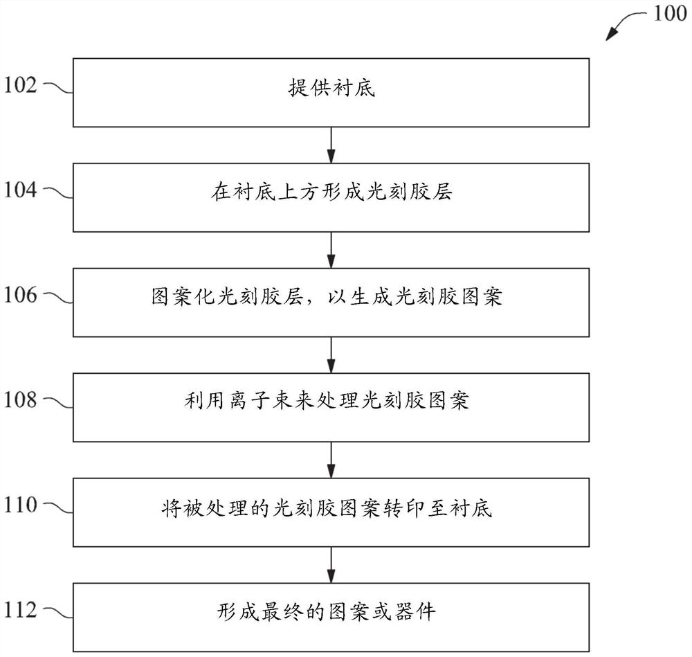
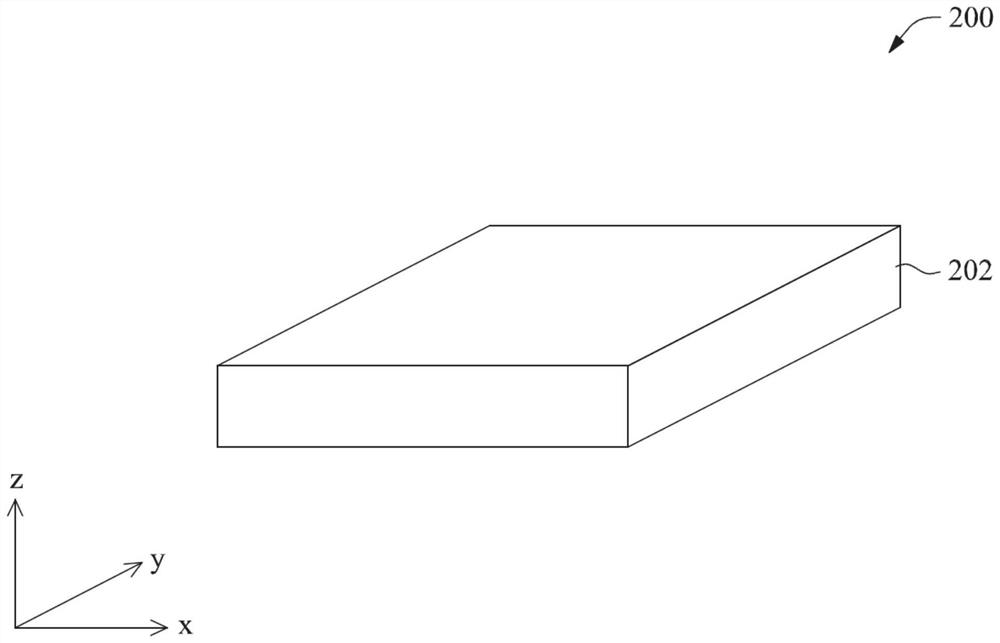
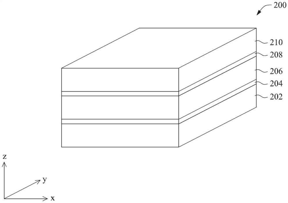
[0034] The following disclosure provides many different embodiments or examples for implementing different features of the presented subject matter. Specific examples of components and arrangements are described below to simplify the present disclosure. Of course, these are examples only and are not intended to be limiting. For example, in the following description, forming a first component over or on a second component may include an embodiment in which the first component and the second component are formed in direct contact, and may also include an embodiment in which the first component and the second component are formed in direct contact. An embodiment in which an additional component may be formed between such that the first component and the second component may not be in direct contact. In addition, the present invention may repeat reference numerals and / or characters in various instances. This repetition is for the purposes of simplicity and clarity and does not i...


PUM

PropertyMeasurementUnit
Twist angleaaaaaaaaaa

Abstract

Provided is a method of patterning a substrate. The method includes patterning a resist layer formed over the substrate to result in a resist pattern and treating the resist pattern with an ion beam.The ion beam is generated with a gas, such as CH4, SiH4, Ar, or He; and is directed towards the resist pattern at a tilt angle at least 10 degrees. In embodiments, the ion beam is directed towards theresist pattern at a uniform twist angle, or at a twist angle having a unimodal or bimodal distribution. The ion beam reduces line edge roughness (LER), line width roughness (LWR), and / or critical dimension of the resist pattern. The method further includes etching the substrate with the treated resist pattern as an etch mask.

Description

[0001] This application is a divisional application of the invention patent application entitled "Method for Patterning Integrated Circuits" with application number 201510530950.X filed on August 26, 2015. [0002] Cross References to Related Applications [0003] This application claims the benefit of US Provisional Patent Application No. 62 / 042,898, filed August 28, 2014, entitled "Method for Integrated Circuit Patterning," the entire contents of which are hereby incorporated by reference. technical field [0004] The present invention generally relates to the field of semiconductor technology, and more particularly, to a method for patterning integrated circuits. Background technique [0005] The semiconductor integrated circuit (IC) industry has undergone rapid development. Technological advances in IC materials and design have produced generations of ICs, where each generation of ICs has smaller and more complex circuits than the previous generation of ICs. In the cou...

Claims


Application Information

Patent Timeline
IPC IPC(8): H01L21/027
CPCH01L21/0279G03F7/40H01L21/0273H01L21/0274H01L21/0275H01L21/26566
Inventor 石志聪游信胜陈政宏严涛南
Owner TAIWAN SEMICON MFG CO LTD
Features
  • R&D
  • Intellectual Property
  • Life Sciences
  • Materials
  • Tech Scout
  • Unparalleled Data Quality
  • Higher Quality Content
  • 60% Fewer Hallucinations
Learn More