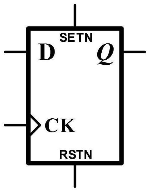
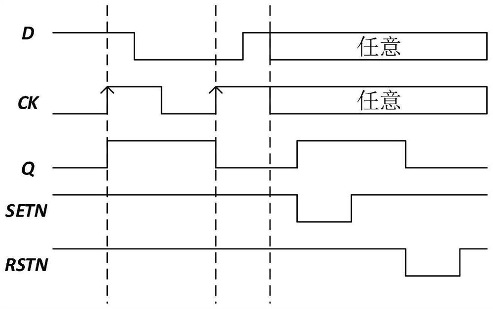
D trigger structure with asynchronous setting reset and rapid output
A set-reset and flip-flop technology, applied in the direction of pulse generation, electrical components, and electric pulse generation, can solve problems affecting the loop speed of the analog-to-digital converter and limit the performance of the analog-to-digital converter, so as to reduce the difficulty of high-speed design , Reduce logic delay, low transmission delay effect
- Summary
- Abstract
- Description
- Claims
- Application Information
AI Technical Summary
Problems solved by technology
Method used
Image

Examples
Embodiment Construction
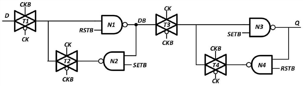
[0026] Such as Figure 2-Figure 4 Shown: a D flip-flop structure with an asynchronous set-reset fast output in this embodiment, including a follower latch circuit, a transmission latch circuit and a feed-forward acceleration circuit;
[0027] The follower latch circuit includes a first transmission gate T1, a sixth transmission gate T6, and a first NOT gate N1 coupled in sequence, and a first feeder is connected in series at both ends of the first NOT gate N1, and the fourth feeder is sequentially coupled to the first feeder. The transmission gate T4, the second conduction node, the second inverting gate N2 and the first PMOS transistor P1, the second conduction node is coupled and connected to the drain of the third PMOS transistor P3 and the drain of the first NMOS transistor M1, and the first The source and drain of the PMOS transistor P1 are connected to the first feeder;
[0028] The transmission latch circuit includes a seventh transmission gate T7, a second transmissio...
PUM
 Abstract
Description
Claims
Application Information
 - R&D
- Intellectual Property
- Life Sciences
- Materials
- Tech Scout
- Unparalleled Data Quality
- Higher Quality Content
- 60% Fewer Hallucinations
Browse by: Latest US Patents, China's latest patents, Technical Efficacy Thesaurus, Application Domain, Technology Topic, Popular Technical Reports.
© 2025 PatSnap. All rights reserved.Legal|Privacy policy|Modern Slavery Act Transparency Statement|Sitemap|About US| Contact US: help@patsnap.com