Chip packaging method
A chip packaging and chip technology, applied in the manufacturing of electrical components, electrical solid-state devices, semiconductor/solid-state devices, etc., can solve problems affecting alignment accuracy, warping, etc., to reduce warping problems and inaccurate alignment. effect of risk
- Summary
- Abstract
- Description
- Claims
- Application Information
AI Technical Summary
Problems solved by technology
Method used
Image

Examples
Embodiment Construction
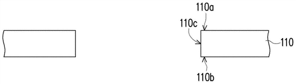
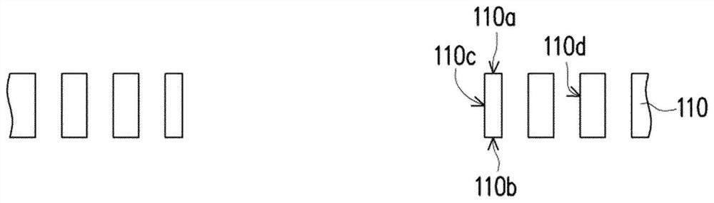
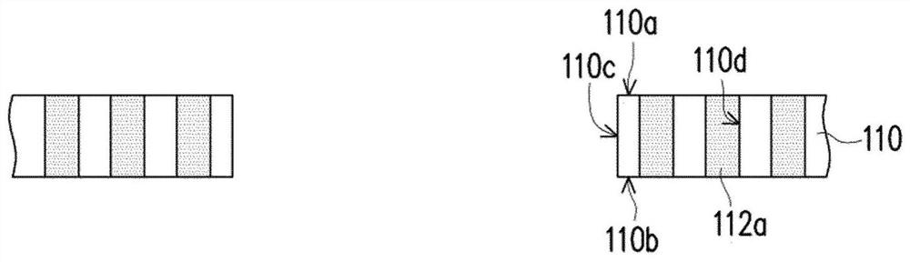
[0043] Please refer to Figure 1A According to the chip packaging method of an embodiment of the present invention, firstly, a support structure 110 is provided. The support structure 110 is integrally formed of the same material, and the support structure 110 has a first support surface 110a, a second support surface 110b opposite to the first support surface 110a, and a connection between the first support surface 110a and the second support surface. A plurality of openings 110c on the surface 110b. In this embodiment, the material of the supporting structure 110 is, for example, metal. In addition, the supporting structure 110 may be a mesh metal structure having a plurality of openings 110c arranged in an array, such as figure 2 As shown, each opening 110c can accommodate corresponding one or more chips.
[0044] Next, carry out the step of forming a plurality of supporting conductive holes 114 (the completed figure will be described later Figure 1E shown). The supp...
PUM
 Abstract
Description
Claims
Application Information
 - R&D
- Intellectual Property
- Life Sciences
- Materials
- Tech Scout
- Unparalleled Data Quality
- Higher Quality Content
- 60% Fewer Hallucinations
Browse by: Latest US Patents, China's latest patents, Technical Efficacy Thesaurus, Application Domain, Technology Topic, Popular Technical Reports.
© 2025 PatSnap. All rights reserved.Legal|Privacy policy|Modern Slavery Act Transparency Statement|Sitemap|About US| Contact US: help@patsnap.com