Method for encapsulating a microelectronic device, comprising a step of thinning the substrate and/or the encapsulation cover
一种微电子器件、封装盖的技术,应用在用于产生装饰表面效果的工艺、半导体/固态器件零部件、电气元件等方向,能够解决制造成本生产时间增加、复杂等问题
- Summary
- Abstract
- Description
- Claims
- Application Information
AI Technical Summary
Problems solved by technology
Method used
Image


Examples
Embodiment Construction
[0043] A method for encapsulating at least one microelectronic device, eg sensitive to air (to oxygen and water vapour), with an encapsulation lid will now be described. The method includes the following sequential steps:
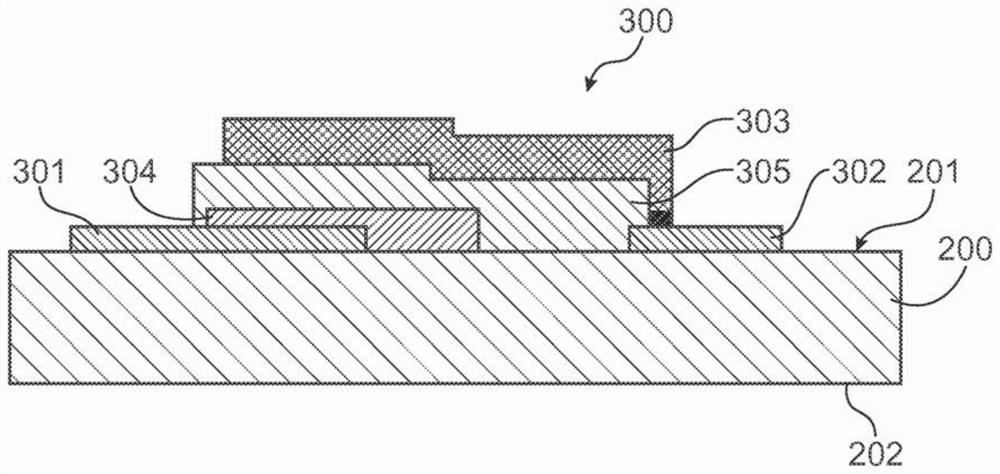
[0044] a) Provide a support substrate 200 made of a first material comprising: a first main surface 201 on which a microelectronic device 300 is arranged, and a second main surface 202 opposite to the first main surface 201 .
[0045] b) Depositing an adhesive layer 500 made of a second material on the first side 201 of the support substrate 200 surrounding the microelectronic device 300 .
[0046] c) Positioning an encapsulation cover 400 made of a third material, comprising a first main face 401 and a second main face 402 opposite to the first main face 401, on the adhesive layer 500, so that the first part of the encapsulation cover 400 The main surface 401 is attached to the carrier substrate 200 and serves to encapsulate the microelectronic component...
PUM
| Property | Measurement | Unit |
|---|---|---|
| coefficient of thermal expansion | aaaaa | aaaaa |
| tensile modulus | aaaaa | aaaaa |
| temperature | aaaaa | aaaaa |
Abstract
Description
Claims
Application Information