Repaired array substrate, repairing method and display panel

An array substrate and repaired technology, applied in the field of liquid crystal display, can solve the problems of bright spot defects and unrepairable bright spot defects, etc.

Pending Publication Date: 2020-09-18
CHENGDU ZHONGDIAN PANDA DISPLAY TECH CO LTD
View PDF8 Cites 1 Cited by
  • Summary
  • Abstract
  • Description
  • Claims
  • Application Information

AI Technical Summary

Problems solved by technology

[0004] However, in the manufacturing process of the array substrate, bright spot defects may be generated in dif

Method used


Image

  • Repaired array substrate, repairing method and display panel
  • Repaired array substrate, repairing method and display panel
  • Repaired array substrate, repairing method and display panel

Examples


Embodiment 1

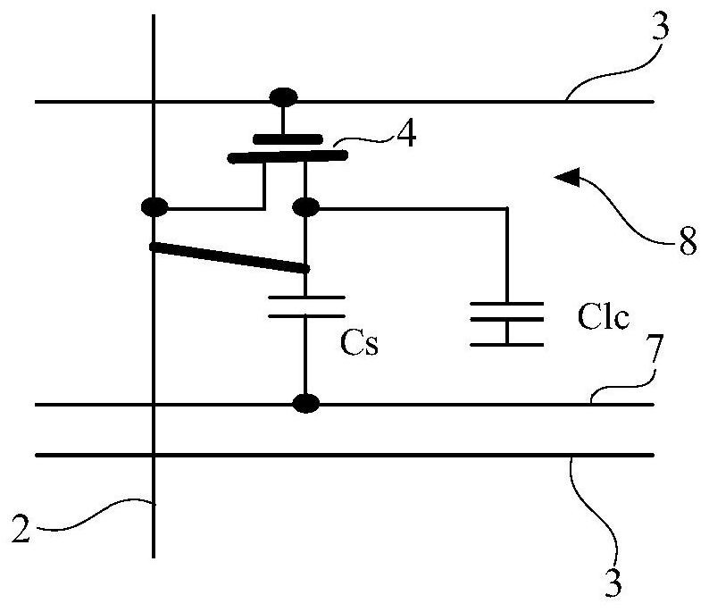
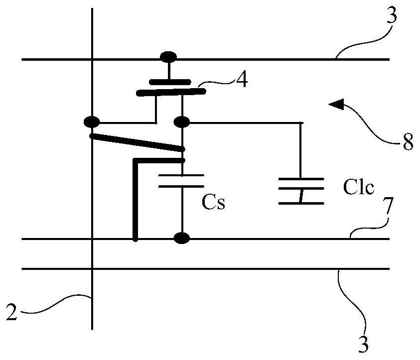
[0051] Figure 5 A schematic structural diagram of an array substrate provided in Embodiment 1 of the present invention; Image 6 A schematic structural diagram of a repaired array substrate provided in Embodiment 1 of the present invention.

[0052] Such as Figure 5 with Image 6 As shown, this embodiment provides an array substrate and a repaired array substrate. The array substrate includes a base substrate 1 and data lines 2 , scan lines 3 and thin film transistors 4 disposed on the base substrate 1 .

[0053] combine Figure 1 to Figure 4 The array substrate firstly includes a base substrate 1 , the base substrate 1 serves as a basic carrying structure of the array substrate, and other functional layers of the array substrate are all formed on the base substrate 1 . Exemplarily, the base substrate 1 may be a glass substrate or a quartz substrate.

[0054] A plurality of data lines 2 and scanning lines 3 are arranged on the base substrate 1, and the data lines 2 are ...

Embodiment 2

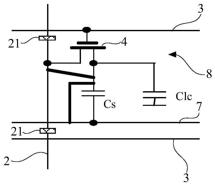
[0087] Figure 7 A schematic flowchart of the method for repairing an array substrate provided in Embodiment 2 of the present invention; Figure 8 A schematic structural diagram of forming an inorganic insulating layer on an active island provided by Embodiment 2 of the present invention; Figure 9 A schematic structural diagram of forming an organic insulating layer on an inorganic insulating layer provided in Embodiment 2 of the present invention; Figure 10 Schematic diagram of the structure of grooves formed in the organic insulating layer provided by Embodiment 2 of the present invention; Figure 11 Schematic diagram of the structure of filling the opaque coating in the groove provided by Embodiment 2 of the present invention; Figure 12 It is a schematic structural diagram of forming a pixel electrode on an organic insulating layer according to Embodiment 2 of the present invention.

[0088] Such as Figure 7 to Figure 12 As shown, this embodiment provides a method f...

Embodiment 3

[0103] This embodiment provides a display panel. The display panel includes a color filter substrate, an array substrate, and a liquid crystal molecular layer sandwiched between the color filter substrate and the array substrate. The array substrate is the array without defect points described in Embodiment 1. The substrate or a repaired array substrate with defects.

[0104] Among them, the structure, function and working principle of the array substrate without defects and the repaired array substrate with defects are described in detail in Embodiment 1, and the repair method for the array substrate with defects can refer to the implementation The method described in Example 2 will not be repeated here.

[0105] Another aspect of this embodiment also provides a display device, including the above-mentioned display panel, the display device may be a flexible display device, wherein, in this embodiment, the display device may be an electronic paper, a tablet computer, a liquid...


PUM

PropertyMeasurementUnit
Thicknessaaaaaaaaaa
Thicknessaaaaaaaaaa

Abstract

The invention provides a repaired array substrate, a repairing method and a display panel. The repaired array substrate comprises a substrate body, data lines, scanning lines and thin film transistors, the data lines, the scanning lines and the thin film transistors are arranged on the substrate body, the data lines and the scanning lines are arranged in a criss-cross mode and define a plurality of pixel areas, and each pixel area is internally provided with the corresponding thin film transistor; the thin film transistor comprises a grid electrode arranged on the substrate and connected withthe scanning line, a grid insulating layer covering the grid electrode, an active island arranged on the grid insulating layer and a passivation layer covering the active island; a groove is formed inthe passivation layer in the pixel area with defect points, and the groove is filled with a lightproof coating, so that the pixel area with the defect points is in a dark spot state through the lightproof coating. The repaired array substrate provided by the invention is suitable for repairing the bright spot defects generated in each production process step, and the repairing structure and the repairing process are relatively simple.

Description

technical field [0001] The invention relates to the technical field of liquid crystal display, in particular to a repaired array substrate, a repair method, and a display panel. Background technique [0002] A liquid crystal display panel is usually composed of an array substrate, a color filter substrate, and a liquid crystal layer sandwiched between the array substrate and the color filter substrate. By applying a driving voltage between the array substrate and the color filter substrate, the liquid crystal layer can be controlled. The liquid crystal molecules rotate to refract the light from the backlight module to produce a picture. [0003] In a liquid crystal display panel, the array substrate is divided by a plurality of data lines and scanning lines criss-crossing to form a plurality of pixel areas arranged in an array, and each pixel area is equipped with a thin film transistor (Thin Film Transistor, referred to as: TFT). The scanning lines provide switching signal...

Claims


Application Information

Patent Timeline
IPC IPC(8): H01L27/12H01L21/77G02F1/1362
CPCH01L27/1214H01L27/1259H01L21/77G02F1/136259G02F1/1362G02F1/136227H01L2021/775
Inventor 前昌弘蒋雷杨宇丹
Owner CHENGDU ZHONGDIAN PANDA DISPLAY TECH CO LTD
Why Eureka
Try Eureka