Display panel, preparation method thereof and display device

A display panel and display area technology, applied in the direction of electrical components, electric solid devices, circuits, etc., can solve the problems of poor bonding between MTD and welding materials, and achieve the effects of solving poor bonding, reducing manufacturing costs, and reducing manufacturing processes

Active Publication Date: 2020-09-18
SHENZHEN CHINA STAR OPTOELECTRONICS SEMICON DISPLAY TECH CO LTD
View PDF6 Cites 2 Cited by
  • Summary
  • Abstract
  • Description
  • Claims
  • Application Information

AI Technical Summary

Problems solved by technology

[0004] The present application provides a display panel, its preparation method, and a display device, which can effectively solve the problem of poor bonding between MTD and welding materials, reduce the display panel manufacturing process, and reduce manufacturing costs

Method used


Image

  • Display panel, preparation method thereof and display device
  • Display panel, preparation method thereof and display device
  • Display panel, preparation method thereof and display device

Examples


Embodiment 1

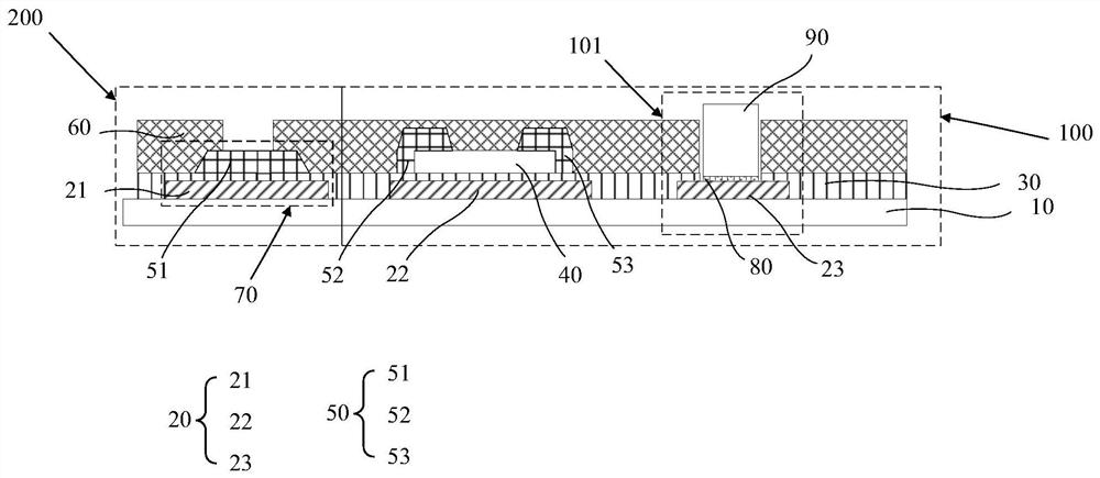
[0040] see figure 1 , a schematic structural diagram of the display panel provided by the embodiment of the present application.

[0041] In this embodiment, the display panel includes a display area 100 and a non-display area 200 surrounding the display area 100 , and the display area 100 includes a plurality of pixel areas 101 .

[0042] The display panel includes a substrate 10; a first electrode layer 20 disposed above the substrate 10; a first insulating layer 30 disposed above the first electrode layer 20; an active layer disposed above the first insulating layer 30 40 ; a second electrode layer 50 disposed above the active layer 40 ; and a second insulating layer 60 disposed above the second electrode layer 50 .

[0043] In this embodiment, the substrate 10 is a PI substrate, mainly polyimide, and the PI material can effectively improve light transmittance.

[0044] In this embodiment, the first electrode layer 20 includes a first electrode 21 , a gate 22 and a weldin...

Embodiment 2

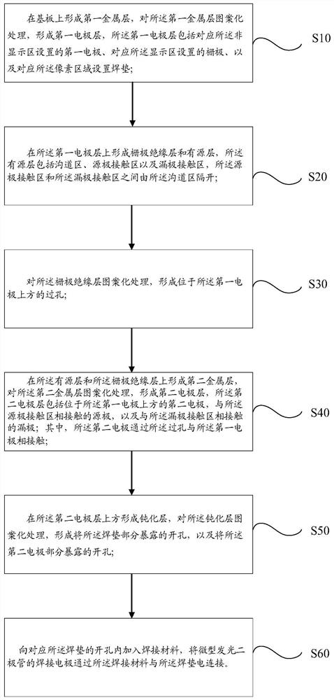
[0076] see image 3 , a flow chart of the steps of the manufacturing method of the display panel provided in the embodiment of the present application.

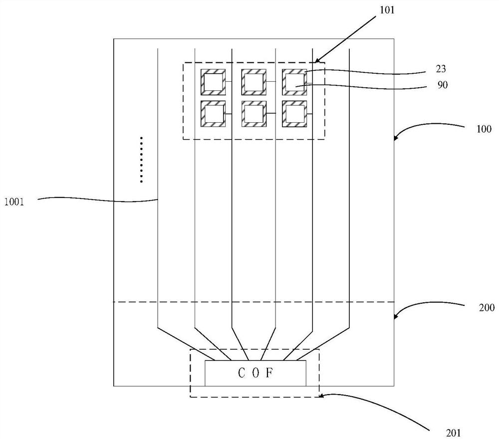
[0077] In this embodiment, the display panel includes a display area 100 and a non-display area 200 surrounding the display area 100 , and the display area 100 includes a plurality of pixel areas 101 .

[0078] The preparation method of the display panel includes:

[0079] Step S10: providing a substrate 10, forming a first metal layer on the substrate 10, patterning the first metal layer to form a first electrode layer 20, the first electrode layer 20 includes The first electrode 21 set at 200, the gate 22 set corresponding to the display area 100, and the pad 23 set corresponding to the pixel area 101, as Figure 4A shown.

[0080] In this embodiment, the substrate 10 is a PI substrate, mainly polyimide, and the PI material can effectively improve light transmittance.

[0081] In this embodiment, the material of the fir...

Embodiment 3

[0098] The present application also provides a display device, which includes the display panel described in Embodiment 1.

[0099] The display panel has been described in detail in Embodiment 1, and the description will not be repeated here.

[0100] The present application provides a display panel, a manufacturing method thereof, and a display device. The display panel includes a display area and a non-display area surrounding the display area, and the display area includes a plurality of pixel areas; the display panel includes a substrate and a The welding pad and the signal line on the substrate, the welding pad is arranged corresponding to the pixel area, and the welding pad is electrically connected to the signal line; the material of the welding pad includes molybdenum / copper laminate, molybdenum At least one of a titanium alloy / copper stack and a titanium-molybdenum-nickel alloy / copper stack; wherein, the welding electrodes on the micro light emitting diodes are electr...


PUM


Abstract

The invention provides a display panel, a preparation method thereof and a display device. The display panel comprises a display area and a non-display area surrounding the display area, and the display area comprises a plurality of pixel areas; the display panel comprises a substrate, a welding pad and a signal line, the welding pad and the signal line are arranged on the substrate, the welding pad is arranged corresponding to the pixel area, and the welding pad is electrically connected with the signal line. Materials of the welding pad comprise at least one of a molybdenum / copper laminationlayer, a molybdenum-titanium alloy / copper lamination layer and a titanium-molybdenum-nickel alloy / copper lamination layer. And the welding electrode on a micro light emitting diode is electrically connected with the welding pad through a welding material. According to the application, the molybdenum / copper laminated material is adopted to prepare the binding welding pad, so that the problem of poor binding force between MTD and the welding material in the prior art can be effectively solved; and meanwhile, the titanium-molybdenum-nickel alloy / copper / titanium-molybdenum-nickel alloy laminationis adopted to prepare a binding lead, so that the manufacturing process of the display panel can be reduced, and the manufacturing cost is reduced.

Description

technical field [0001] The present application relates to the field of display technology, in particular to a display panel, a manufacturing method thereof, and a display device. Background technique [0002] Mini / Micro LED (MLED) display technology has entered a stage of accelerated development in the past two years, and can be used in small and medium-sized high value-added display applications. Compared with OLED screens, MLED displays can show better performance in terms of cost, contrast ratio, high brightness and thin and light appearance. [0003] In MLED display technology, backplane technology is the key technology, optimizing backplane technology is very important for MLED display technology, while the conventional BCE_TFT backplane technology adopts 6mask technology, in which M2 uses Mo / Cu metal as LED bonding Pad, and ITO as COF Bonding protective layer to prevent Cu oxidation; however, the process temperature window of this technology is low, and the increase o...

Claims


Application Information

Patent Timeline
Patent Type & Authority Applications(China)
IPC IPC(8): H01L27/15H01L33/62
CPCH01L27/156H01L33/62H01L2933/0066H01L25/0753H01L25/167H01L33/40H01L2933/0016
Inventor 梅雪茹卢马才
Owner SHENZHEN CHINA STAR OPTOELECTRONICS SEMICON DISPLAY TECH CO LTD
Why Eureka
Try Eureka