


Quick Research
Generate reliable direction feasibility study reports for your R&D in just a few steps.

Technical Q&A
Discover and master advanced knowledge NOW. Basics, ideas, possibilities, all at once.

Find Solutions
As an expert in R&D theories, this can generate solutions to your technical problems instantly.

Evaluate Feasibility
Analyze your overall solution with one click, know your potential R&D risks in advance.

Monitor Landscape
Get weekly tech updates, stay abreast of the latest tech innovations and key insights.
Chip testing method and device
A chip test and chip technology, applied in the field of information processing, can solve the problems of CP test efficiency to be improved, and achieve the effect of improving efficiency, increasing test frequency, and increasing output speed
- Summary
- Abstract
- Description
- Claims
- Application Information
AI Technical Summary
Problems solved by technology
Method used
Image

Examples
Embodiment Construction
[0021] In order to make the purpose, technical solutions and advantages of the embodiments of the present application clearer, the embodiments of the embodiments of the present application will be described in detail below with reference to the accompanying drawings. It should be noted that, in the case of no conflict, the embodiments in the embodiments of the present application and the features in the embodiments can be combined arbitrarily with each other.
[0022] During the process of implementing this application, the inventor conducted a technical analysis on the related technology, and found that the related technology had at least the following problems, including:
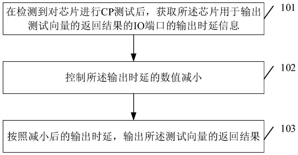
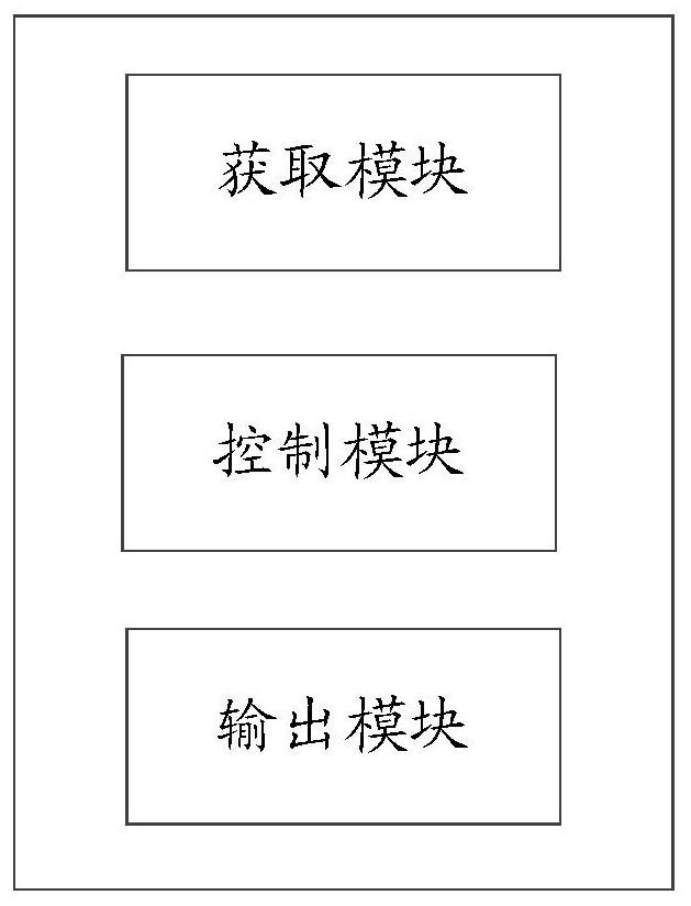
[0023] The CP machine test mainly works at about 10MHz. It is not that the CP machine cannot provide a higher frequency clock. The main reason depends on the communication speed of the integrated circuit chip IO, because the IO communication speed of the integrated circuit chip is slow in the return phase....
PUM
 Abstract
Description
Claims
Application Information
 - R&D Engineer
- R&D Manager
- IP Professional
- Industry Leading Data Capabilities
- Powerful AI technology
- Patent DNA Extraction
Browse by: Latest US Patents, China's latest patents, Technical Efficacy Thesaurus, Application Domain, Technology Topic, Popular Technical Reports.
© 2024 PatSnap. All rights reserved.Legal|Privacy policy|Modern Slavery Act Transparency Statement|Sitemap|About US| Contact US: help@patsnap.com