

display panel
A display panel and display area technology, applied in the direction of identification devices, instruments, etc., can solve the problem of small stress in the bending area
- Summary
- Abstract
- Description
- Claims
- Application Information
AI Technical Summary
Problems solved by technology
Method used
Image

Examples
Embodiment 1
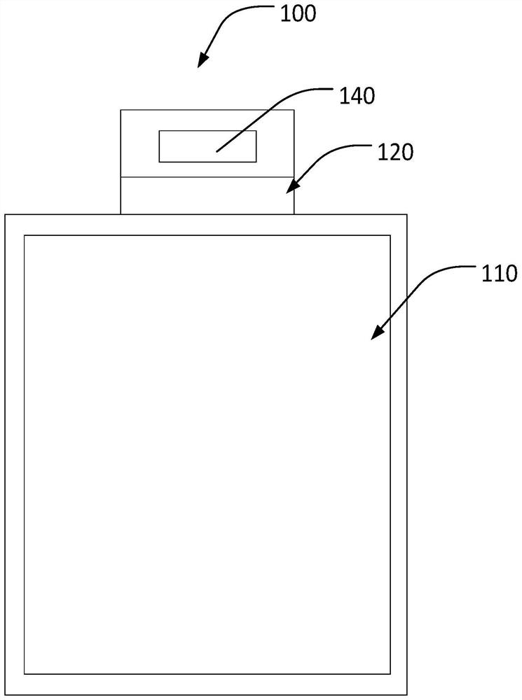
[0030] Such as Figure 1~3 As shown, Embodiment 1 of the present invention provides a display panel 100 , including: a base substrate 101 , a barrier layer 102 and a driving circuit layer 130 .
[0031] The base substrate 101 includes a display area 110 and a non-display area, and the non-display area includes a bending sub-area 120 . The barrier layer 102 is disposed on the base substrate 101 , and the driving circuit layer 130 is disposed on the barrier layer 102 .
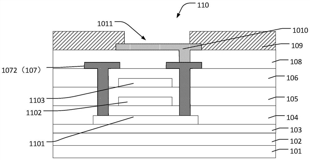
[0032] The driving circuit layer 130 includes: a buffer sublayer 103, an active sublayer 1101, a first insulating sublayer 104, a first metal sublayer 1102, a second insulating sublayer 105, a second metal sublayer 1103, and an interlayer insulating sublayer 106 .
[0033] The buffer sublayer 103 is disposed on one side of the base substrate 101 .
[0034] The active sublayer 1101 is disposed on a side of the buffer sublayer 103 away from the base substrate 101 . The material of the active layer 1101 is poly...
Embodiment 2
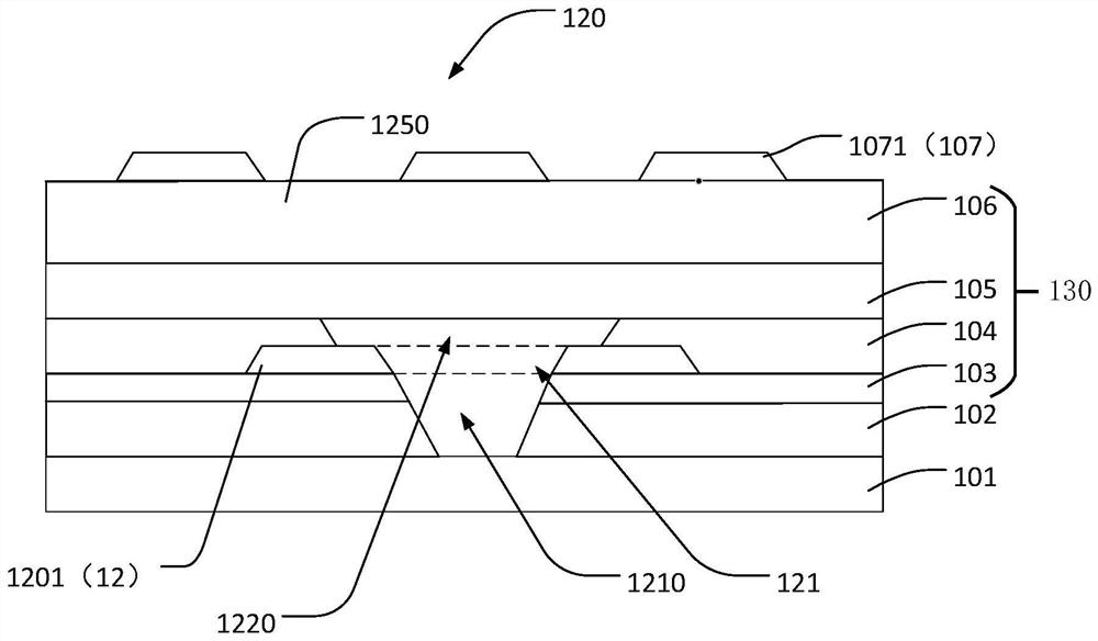
[0064] Such as Figure 4 As shown, Embodiment 2 of the present invention provides a display panel 100a, which is different from Embodiment 1 in that, in the bending sub-region 120a, the driving circuit layer 130a includes at least two etching stop sub-layers 12a, namely The first etch stop sublayer 1201a and the second etch stop sublayer 1202a.
[0065] There is a gap between the two etch stop sublayers 12a adjacent up and down, and the projections on the base substrate 101a overlap, and the opening width of the etch stop sublayer away from the base substrate 101a is larger than that close to the substrate. The opening width of the etch stop sublayer of the base substrate 101a.
[0066] Specifically, two adjacent etch stop sub-layers 12a are formed in different insulating layers. The etch stop sublayer 12a includes a first etch stop sublayer 1201a and a second etch stop sublayer 1202a, the first etch stop sublayer 1201a is formed in the first insulating sublayer 104a, the T...
Embodiment 3
[0075] Such as Figure 5 As shown, Embodiment 3 of the present invention provides a display panel 100b. The difference from Embodiment 2 is that the etch stop sublayer 12b includes a first etch stop sublayer 1201b, a second etch stop sublayer 1202b , and the third etch stop sublayer 1203b. That is, the number of etch stop sub-layers 12b includes 3 layers.
[0076] Specifically, two adjacent etch stop sub-layers 12b are formed in different insulating layers. The etch barrier sublayer 12b includes a first etch barrier sublayer 1201b, a second etch barrier sublayer 1202b and a third etch barrier sublayer 1203b, the first etch barrier sublayer 1201b is formed with the In the first insulating sublayer 104b, the second etch stop sublayer 1202b is formed in the second insulating sublayer 105b, and the third etch stop sublayer 1203b is formed in the interlayer insulating sublayer 106b.
[0077] The first etch stop sublayer 1201b has a first opening 121b and is disposed on the first...
PUM
 Abstract
Description
Claims
Application Information