PCB processing method based on crimping holes and PCB

A technology of PCB board and processing method, applied in the field of PCB design, can solve the problem that the space occupied by holes is not used and so on

Inactive Publication Date: 2020-10-27
SUZHOU LANGCHAO INTELLIGENT TECH CO LTD
View PDF4 Cites 0 Cited by
  • Summary
  • Abstract
  • Description
  • Claims
  • Application Information

AI Technical Summary

Problems solved by technology

However, the effective contact distance of the hole may not be from the top to the bottom surface, such as figure 1 As shown, the lower half of the hole is not connected to other layers, and the space occupied by the hole in this part is not used

Method used


Image

  • PCB processing method based on crimping holes and PCB
  • PCB processing method based on crimping holes and PCB
  • PCB processing method based on crimping holes and PCB

Examples


Embodiment 1

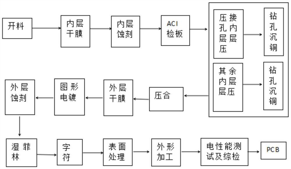
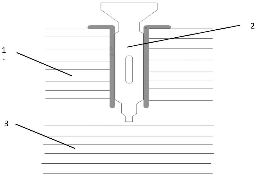
[0035] Please refer to figure 2 , the present embodiment provides a PCB board processing method based on crimping holes, comprising the following steps:

[0036] S1. Set the position information of the crimping hole on the PCB design graphic, and calibrate the effective layer of the crimping hole. The effective layers of the crimping hole in this embodiment are all three upper surface layers. The lower half area except the effective layer can be normally designed for routing, and the routing does not need to bypass the position of the crimping hole.

[0037] S2. Firstly, process the material cutting, memory dry film, memory etching and ACI board inspection process for each layer of the PCB board. The effective layer is laminated into the first sub-board, and copper is drilled on the first sub-board, and the size of the drill hole matches the pin of the crimper. According to the PCB design pattern, press the lower half of the PCB board to obtain the second sub-board, and dr...

Embodiment 2

[0040] This embodiment provides a PCB board processing method based on crimping holes, comprising the following steps:

[0041] Compared with Example 1, if the number of effective layers of PCB holes is different, the method of splicing and stacking is used to prepare the PCB. For example, there are two kinds of drill holes, drill hole 1 is the third floor in the upper half area, and drill hole 2 is the fifth floor in the upper half area. Firstly, press the three-layer boards in the upper half area to obtain the first sub-board, and drill holes at the corresponding positions of the drilling holes 1 on the first sub-board. The remaining two layers of the drilled hole 2 are superimposed and pressed on the first sub-board to obtain a second sub-board, and copper sinking is performed on the corresponding position of the drilled hole 2 of the second sub-board.

Embodiment 3

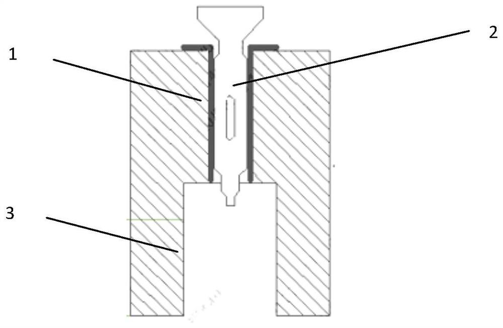
[0043] Please refer to image 3 , this embodiment provides a PCB board. The crimping hole of the PCB board provided in this embodiment is only drilled on the effective layer, and the hole matches the pin size of the crimping device. There are no drill holes on the board layer of the PCB board that is not in contact with the pins of the crimper, and the wiring can be routed normally.


PUM


Abstract

The invention provides a PCB processing method based on crimping holes and a PCB. The method comprises the steps of setting the position information of the crimping holes in a PCB design pattern, andcalibrating effective layers of the crimping holes; laminating the effective layers into a first daughter board according to the PCB design pattern, and drilling holes in corresponding positions of the first daughter board according to the position information; laminating the PCB layers except the effective layers into a second daughter board; and laminating the first daughter board and the seconddaughter board into the PCB. According to the invention, the wiring space of the PCB is improved, the wiring in the lower half area does not need hole winding, and the wiring difficulty is reduced.

Description

technical field [0001] The invention belongs to the technical field of PCB design, and in particular relates to a method for processing a PCB board based on crimping holes and the PCB board. Background technique [0002] As a key component in the signal transmission process, connectors are widely used on PCB circuit boards. The connector and the PCB board are mainly welded together through the metal pins on the connector and the holes on the PCB board, or combined by extrusion. The holes on the PCB board are designed as through-holes. From the board The upper surface passes through to the lower surface. However, the effective contact distance of the hole may not be from the top to the bottom surface, such as figure 1 As shown, the lower half of the hole is not connected to other layers, and the space occupied by the hole in this part is not used. Contents of the invention [0003] In view of the above-mentioned deficiencies in the prior art, the present invention provid...

Claims


Application Information

Patent Timeline
IPC IPC(8): H05K3/46H05K3/00
CPCH05K3/0047H05K3/4638
Inventor 司云
Owner SUZHOU LANGCHAO INTELLIGENT TECH CO LTD
Why Eureka
Try Eureka