Check patentability & draft patents in minutes with Patsnap Eureka AI!

Wafer curvature measuring method and device and storage medium

A measurement method and a curvature technology, applied in the field of wafer curvature measurement, can solve the problems of inability to realize online measurement, expensive wafer curvature measurement device, etc., and achieve the effect of online measurement, low cost, and low measurement cost.

Inactive Publication Date: 2020-11-03
YANGTZE MEMORY TECH CO LTD
View PDF4 Cites 0 Cited by
  • Summary
  • Abstract
  • Description
  • Claims
  • Application Information

AI Technical Summary

Problems solved by technology

[0003] However, the wafer bow measurement device in the related art is expensive, and at the same time, online measurement cannot be realized when using the wafer bow measurement device in the related art to measure the wafer bow

Method used


Image

  • Wafer curvature measuring method and device and storage medium
  • Wafer curvature measuring method and device and storage medium
  • Wafer curvature measuring method and device and storage medium

Examples


Embodiment Construction

[0041] In order to make the technical solutions and advantages of the embodiments of the present invention more clear, the specific technical solutions of the invention will be further described in detail below in conjunction with the drawings in the embodiments of the present invention.

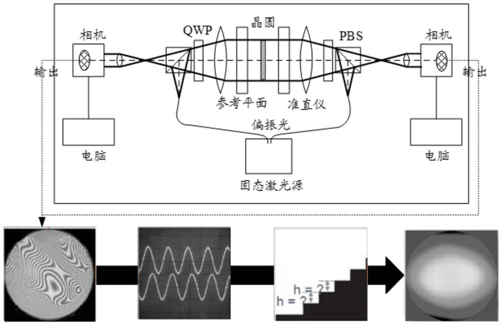
[0042] In the related art, when wafer measurement is performed, the wafer is generally taken out from the corresponding semiconductor processing equipment after the wafer has completed the corresponding semiconductor process, and put into the relevant wafer bow measurement device, and the warped wafer is measured. Wafers are tested directly. At present, there are mainly two test devices with different measurement principles. The first one: PWG. PWG is a machine produced by KLATencor (Ke Lei) Company that uses the principle of white light interference to measure wafer deformation. The measurement principle of this machine is as follows: Figure 1a As shown, the solid-state laser source emits p...


PUM


Abstract

The embodiment of the invention provides a wafer curvature measuring method and device and a storage medium, and the method comprises the steps: measuring the stress of the back surface of a wafer through a strain testing device, wherein the strain testing device is arranged on the back surface of the wafer, and the strain testing device carries out a semiconductor processing technology along withthe wafer; and obtaining the curvature of the wafer by utilizing the measured stress and combining the corresponding relationship between the stress and the curvature of the wafer. Thus, when the wafer curvature is measured, the measurement cost is low, and online measurement can be realized.

Description

technical field [0001] The invention relates to the technical field of semiconductors, in particular to a wafer bow measurement method. Background technique [0002] In the semiconductor manufacturing process, a series of processes need to be performed on the front of the wafer, such as thin film deposition, etching, etc. These processes will cause the wafer to bend, and the wafer curvature (expressed in English as bow ) too large will lead to a series of bad consequences. Therefore, it is of great significance to measure the curvature of the wafer to provide data support for adjusting the curvature of the wafer. [0003] However, the wafer bow measurement device in the related art is expensive, and at the same time, online measurement cannot be realized when using the wafer bow measurement device in the related art to measure the wafer bow. Contents of the invention [0004] In order to solve related technical problems, embodiments of the present invention provide a met...

Claims


Application Information

Patent Timeline
IPC IPC(8): H01L21/66
CPCH01L22/12H01L22/20
Inventor 王凡
Owner YANGTZE MEMORY TECH CO LTD
Features
  • R&D
  • Intellectual Property
  • Life Sciences
  • Materials
  • Tech Scout
  • Unparalleled Data Quality
  • Higher Quality Content
  • 60% Fewer Hallucinations
Learn More