Array substrate, manufacturing method thereof and display device

A technology of array substrate and display area, which is applied in semiconductor/solid-state device manufacturing, optics, instruments, etc., and can solve problems such as poor display

Pending Publication Date: 2020-11-06
CHUZHOU HKC OPTOELECTRONICS TECH CO LTD +1
View PDF10 Cites 12 Cited by
  • Summary
  • Abstract
  • Description
  • Claims
  • Application Information

AI Technical Summary

Problems solved by technology

[0004] Based on this, it is necessary to provide an array substrate, a manufacturing method thereof, and a display device for the problem of poor display caused by laser cutting.

Method used


Image

  • Array substrate, manufacturing method thereof and display device
  • Array substrate, manufacturing method thereof and display device
  • Array substrate, manufacturing method thereof and display device

Examples


Embodiment Construction

[0029] In order to make the above objects, features and advantages of the present invention more comprehensible, specific implementations of the present invention will be described in detail below in conjunction with the accompanying drawings. In the following description, numerous specific details are set forth in order to provide a thorough understanding of the present invention. However, the present invention can be implemented in many other ways different from those described here, and those skilled in the art can make similar improvements without departing from the connotation of the present invention, so the present invention is not limited by the specific implementations disclosed below.

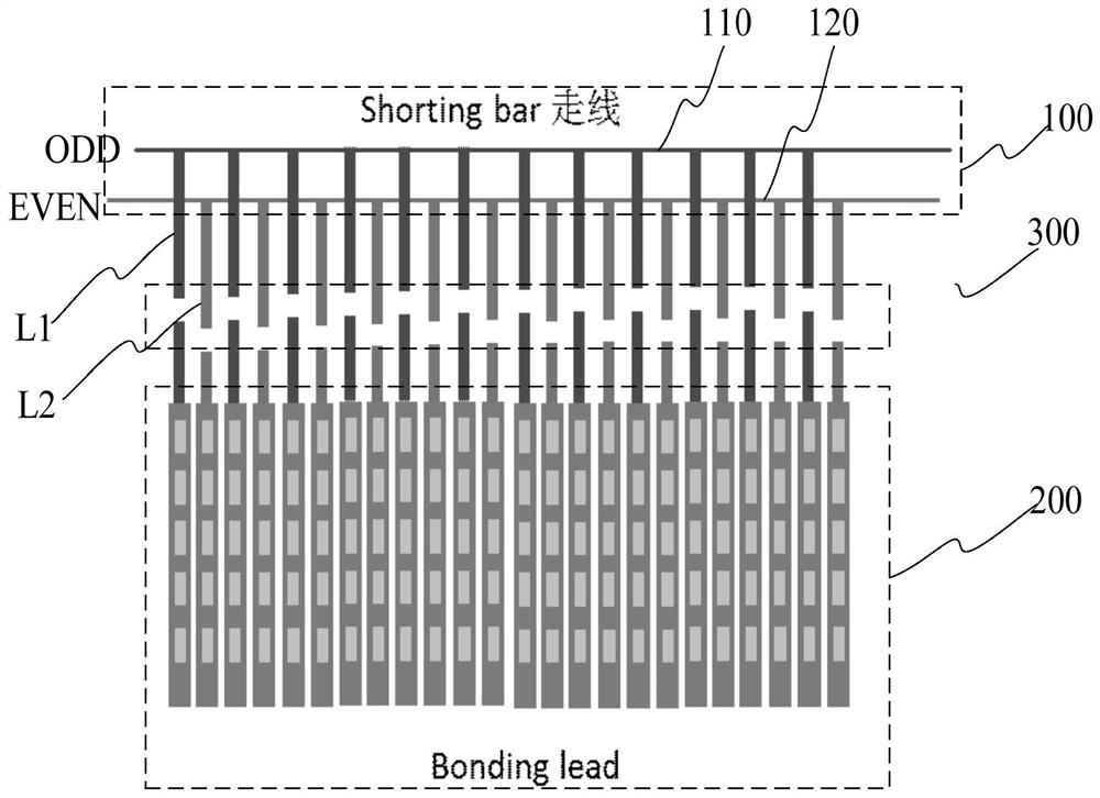
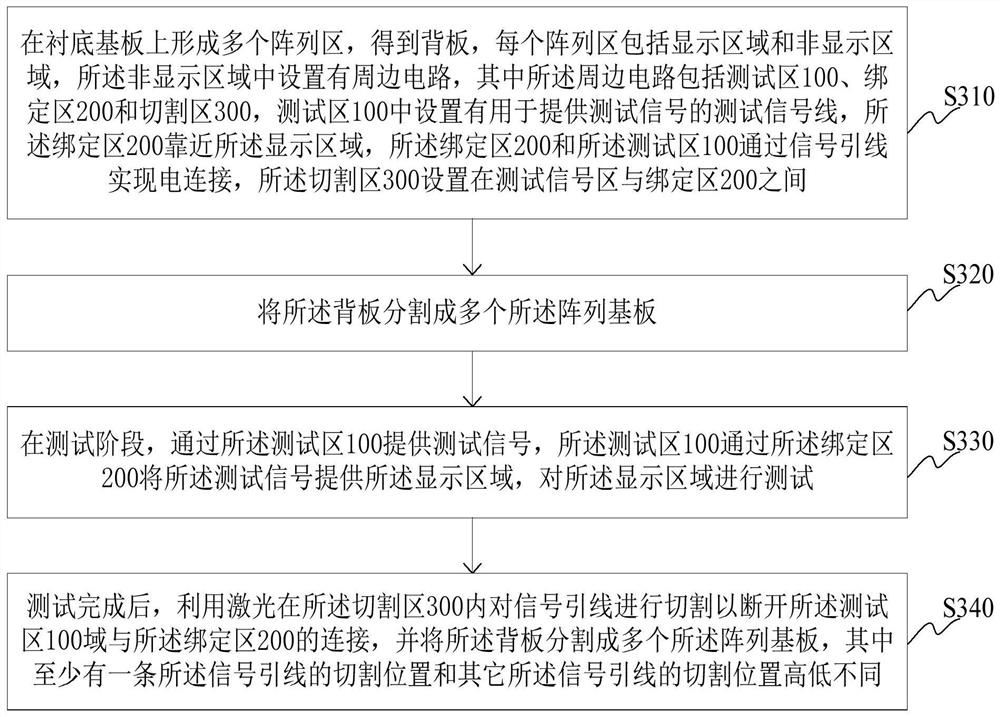
[0030] See figure 1 , an embodiment of the present invention provides an array substrate, the array substrate includes a display area and a non-display area, the non-display area is provided with a peripheral circuit, wherein the peripheral circuit includes a test area 100, a binding ...


PUM


Abstract

The invention relates to an array substrate, a manufacturing method thereof and a display device. The array substrate comprises a display area and a non-display area. A peripheral circuit is arrangedin the non-display area, and the peripheral circuit comprises a test area, a binding area and a cutting area. A test signal line is arranged in the test area and used for providing a test signal. Thebinding area is close to the display area, and the binding area and the test area are electrically connected through a signal lead. The cutting area is arranged between the test signal area and the binding area. After finishing a cutting process in the cutting area, a cutting opening is formed in each signal lead, wherein the position of the cutting port of at least one signal lead is different from the positions of the cutting ports of other signal leads. Therefore, the distance between the cutting openings of the two adjacent signal leads is increased, the possibility that the two adjacent signal leads are connected together through metal chippings is reduced, the problem of short circuit between the two adjacent signal leads caused by laser cutting is avoided, and the yield of the panelis improved.

Description

technical field [0001] The invention relates to the technical field of liquid crystal display, in particular to an array substrate, a manufacturing method thereof, and a display device. Background technique [0002] In the manufacturing process of the display panel, multiple testing procedures are required, and one of the important testing procedures is to conduct a lighting test by lighting a lamp before the chip-on-film packaging. After the test is completed, the signal leads between the shorting bar and the test signal line need to be disconnected by laser cutting. [0003] However, during the laser cutting process, metal debris will accumulate at the fracture site of the metal. Once the metal debris accumulates too much, there will be a problem of short circuit between two adjacent signal leads, which will cause abnormal display of the panel and reduce the yield rate of the display panel. Contents of the invention [0004] Based on this, it is necessary to provide an...

Claims


Application Information

Patent Timeline
Patent Type & Authority Applications(China)
IPC IPC(8): H01L27/12H01L21/77G02F1/1362
CPCH01L27/1244H01L27/1259G02F1/136286
Inventor 黄世帅李伟
Owner CHUZHOU HKC OPTOELECTRONICS TECH CO LTD
Why Eureka
Try Eureka