Electronic carrier board

A carrier board and electronic technology, which is applied in the direction of electrical components, electrical components, printed circuits, etc., can solve the problems of unequal wetted areas, inability to use, and low resolution of photosensitive solder mask, so as to avoid different pad areas Effect

Inactive Publication Date: 2007-08-01
SILICONWARE PRECISION IND CO LTD
View PDF2 Cites 14 Cited by
  • Summary
  • Abstract
  • Description
  • Claims
  • Application Information

AI Technical Summary

Problems solved by technology

[0015] This technology is still limited by the low resolution of the photosensitive solder mask layer. When the limited pad spacing is less than 275 microns, it is impossible to form barrier strips 331, so it cannot be applied to 0201 passive components.
[0016] In addition, when the solder mask layer is offset, the wetting area of ​​the two solder pads will be unequal. As shown in Figure 3B, the area of ​​the original solder pad that can be soldered (exposed solder mask layer opening area ) is A*B, if the solder mask is shifted to the left by X microns (the traditional substrate process offset capability is 75 microns), the area of ​​the left pad will be B*(A+X), and the area of ​​the right pad will be B*(A-X), the area of ​​the two pads will have a difference of B*(A+X)-B*(A-X)=2BX, this different wetted area will lead to passive components soldered on the pad Tombstone occurs
[0017] Furthermore, in the technologies disclosed in the above-mentioned U.S. Patent No. 6,521,997 and No. 2005/0253231, in

Method used


Image

  • Electronic carrier board
  • Electronic carrier board
  • Electronic carrier board

Examples


Embodiment 1

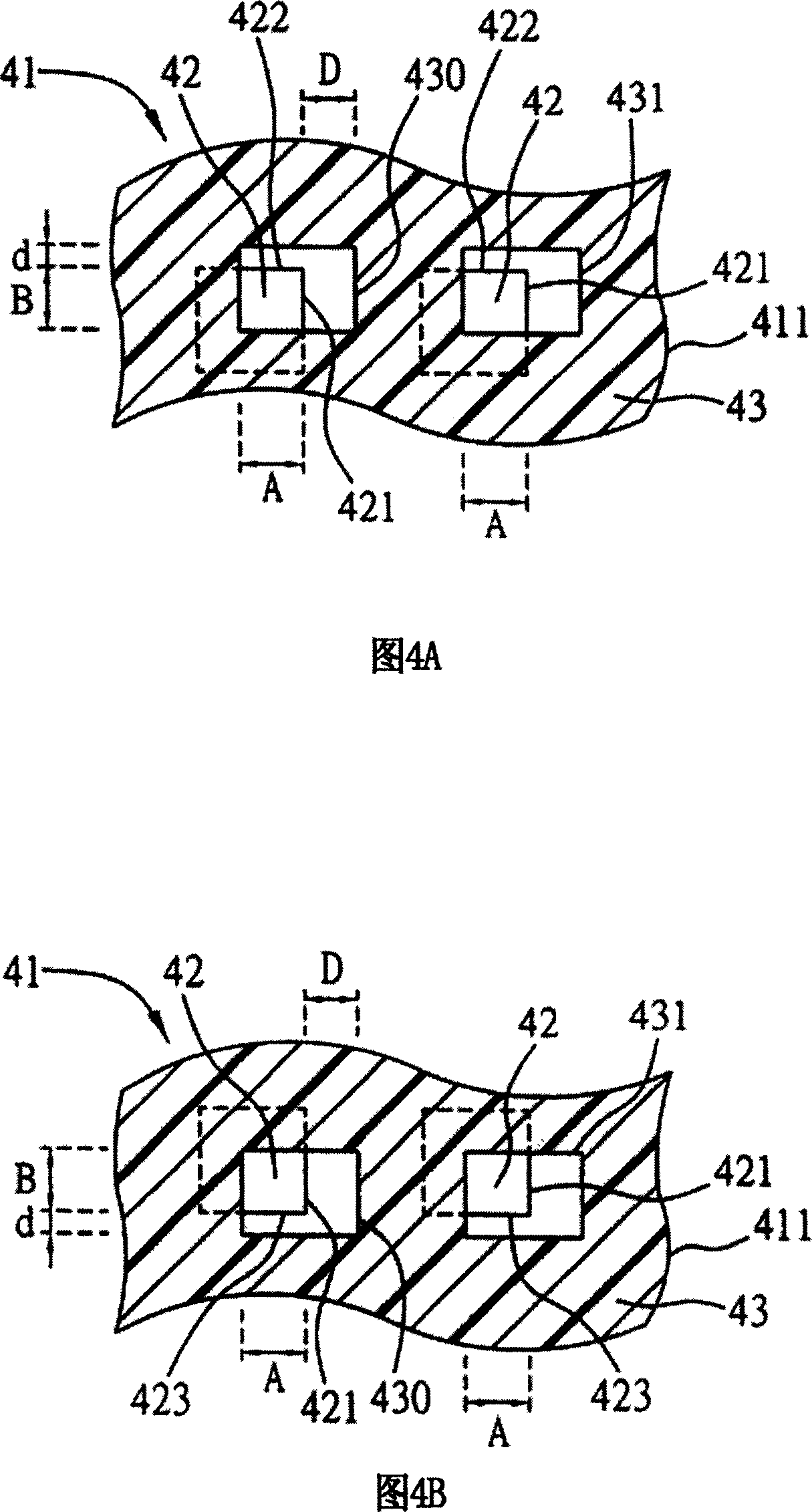
[0051] Please refer to FIG. 4A and FIG. 4B , which are schematic plan views of Embodiment 1 of the electronic carrier board of the present invention.

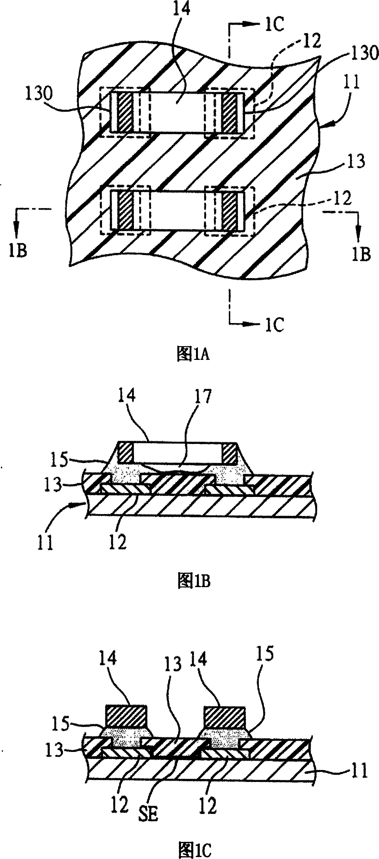
[0052] The electronic carrier board of the present invention comprises: a main body 411; at least two welding pads 42 arranged in pairs on the surface of the main body 411; and a protective layer 43 for covering the surface of the main body, the protective layer 43 corresponding to the two Openings 430 and 431 are formed at the position of the first welding pad 42. The openings 430 and 431 are in the same direction as each other and expose two identical first side walls 421 of the second welding pad 42 with a width of B and the first side wall 421 of the width A. The two side walls 422 (or the third side wall 423) form a pair of welding pads whose exposed area is A*B. The first side wall 421 of the welding pad is arranged vertically to the pair of welding pads 42. The direction of the second side wall 422 (or the third side wal...

Embodiment 2

[0058] Please refer to FIG. 5 , which is a schematic plan view of Embodiment 2 of the electronic carrier board of the present invention.

[0059] The electronic carrier board of Embodiment 2 of the present invention is substantially the same as the above-mentioned Embodiment 1, the main difference is that the protective layer 43 on the electronic carrier board 41 is corresponding to at least two openings 430 and 431 formed between the welding pads 42 arranged in pairs, The openings 430 and 431 are in the same direction as each other and expose three identical first sidewalls 421, second sidewalls 422 and third sidewalls 423 of the two welding pads 42. The first sidewalls 421 of the welding pads are vertical. The direction in which the pair of welding pads 42 are arranged, the second sidewall 422 and the third sidewall 423 are parallel to the direction in which the pair of welding pads 42 are arranged, and the distance D between the first sidewall 421 and the openings 430 and 43...

Embodiment 3

[0063] Please refer to FIG. 6A , which is a schematic plan view of Embodiment 3 of the electronic carrier board of the present invention.

[0064] The electronic carrier board of Embodiment 3 of the present invention is substantially the same as the above-mentioned Embodiment 1, the main difference is that the protective layer 43 on the electronic carrier board 41 is corresponding to at least two openings 430 and 431 formed between the welding pads 42 arranged in pairs, The openings 430 and 431 are in the same direction as each other and fully expose the same first sidewall 421, second sidewall 422, third sidewall 423 and fourth sidewall 424 of the two pads 42, wherein the first, second sidewall 423 and fourth sidewall 424 are identical. The fourth sidewalls 421, 424 are perpendicular to the direction in which the pair of welding pads 42 are arranged, the second and third sidewalls 422, 423 are parallel to the direction in which the pair of welding pads 42 are arranged, and the...


PUM


Abstract

The disclosed electric carrier plate comprises: a main body, at least two welding mats set on body surface in pairs, a protective layer covering body surface and forming an opening opposite to the mat position, wherein there are at least two same side walls on the opening to expose the mats, the first one is set vertically to the mat arrangement direction, while the second one is parallel. This invention can avoid different area of exposed mats, prevents electric element standing on the plate, fills insulation material between element and plate efficiently, and overcomes problem that it cannot form flow-in groove for package resin on small-size passive element bottom.

Description

technical field [0001] The present invention relates to an electronic carrier board, in particular to an electronic carrier board applied in surface mount technology (Surface Mounted Technology, SMT). Background technique [0002] With the advancement of integrated circuit production technology, the design and production of electronic components continue to develop towards the trend of miniaturization, and because they have larger-scale and highly integrated electronic circuits, their product functions are also more complete. [0003] In this case, the electronic components that are traditionally placed using Through Hole Technology (Through Hole Technology; THT) cannot be further reduced in size, thus occupying such as printed circuit board (Printed Circuit Board; PCB), circuit board (circuitboard) ) or substrate (substrate) and other electronic carrier boards have a lot of space, and the plug-in assembly technology needs to drill holes on the electronic carrier board corre...

Claims


Application Information

Patent Timeline
IPC IPC(8): H05K1/00H05K13/00
Inventor 蔡芳霖蔡和易曾文聪黄致明
Owner SILICONWARE PRECISION IND CO LTD
Why Eureka
Try Eureka