Printed circuit board and its processing method, device, and electronic equipment
A technology of printed circuit board and processing method, applied in the field of communication, can solve the problems of poor use reliability of communication products, and achieve the effect of ensuring the use reliability
- Summary
- Abstract
- Description
- Claims
- Application Information
AI Technical Summary
Problems solved by technology
Method used
Image

Examples
Embodiment Construction
[0024] In order to facilitate the understanding of the present application, the present application will be described more fully below with reference to the relevant drawings. Preferred embodiments of the application are shown in the accompanying drawings. However, the present application can be embodied in many different forms and is not limited to the embodiments described herein. On the contrary, the purpose of providing these embodiments is to make the understanding of the disclosure of the application more thorough and comprehensive.
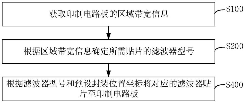
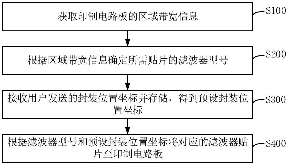
[0025] see figure 1 , a method for processing a printed circuit board, comprising step S100, step S200 and step S400.
[0026] Step S100, acquiring area bandwidth information of the printed circuit board.
[0027] Specifically, the area bandwidth information represents the communication bandwidth corresponding to the area where the printed circuit board is used. In modern communication technology, the communication bandwidth required by...
PUM
 Abstract
Description
Claims
Application Information
 - R&D
- Intellectual Property
- Life Sciences
- Materials
- Tech Scout
- Unparalleled Data Quality
- Higher Quality Content
- 60% Fewer Hallucinations
Browse by: Latest US Patents, China's latest patents, Technical Efficacy Thesaurus, Application Domain, Technology Topic, Popular Technical Reports.
© 2025 PatSnap. All rights reserved.Legal|Privacy policy|Modern Slavery Act Transparency Statement|Sitemap|About US| Contact US: help@patsnap.com