Check patentability & draft patents in minutes with Patsnap Eureka AI!

A Test Structure for Dielectric Layer Defect Detection

A technology for testing structure and defect detection, which is applied in short-circuit testing, single semiconductor device testing, semiconductor/solid-state device testing/measurement, etc., and can solve the problem that testing items cannot share the same testing structure.

Active Publication Date: 2021-01-01
晶芯成(北京)科技有限公司
View PDF5 Cites 0 Cited by
  • Summary
  • Abstract
  • Description
  • Claims
  • Application Information

AI Technical Summary

Problems solved by technology

[0005] The purpose of the present invention is to provide a test structure for dielectric layer defect detection, which can solve the problem that the detection items required by different leakage thresholds cannot share the same test structure, and can also reduce the area occupied by the test structure for dielectric layer defect detection. , to improve the flexibility of the test structure during testing

Method used


Image

  • A Test Structure for Dielectric Layer Defect Detection
  • A Test Structure for Dielectric Layer Defect Detection
  • A Test Structure for Dielectric Layer Defect Detection

Examples


Embodiment Construction

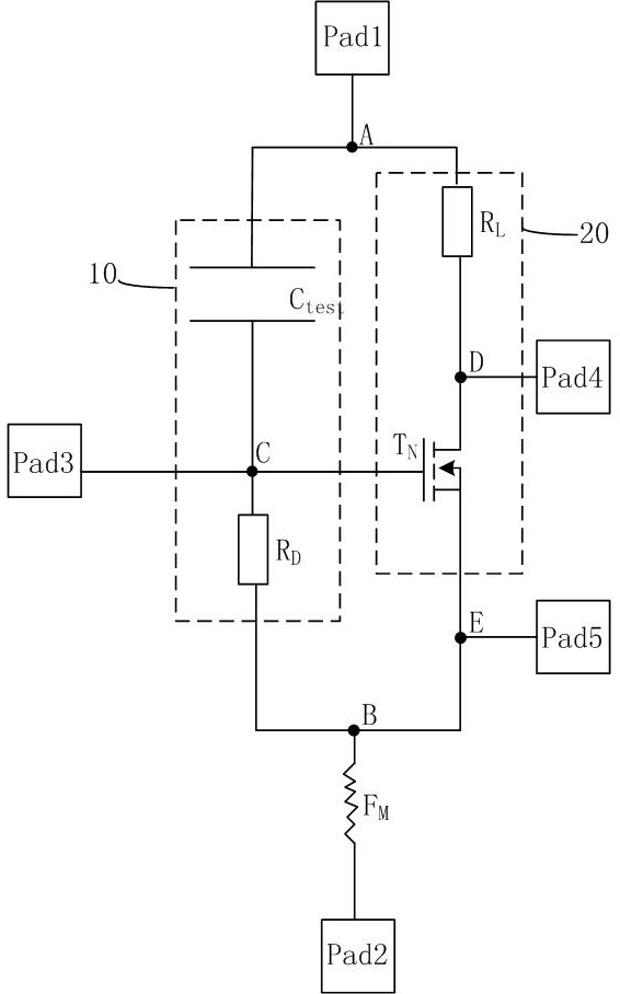
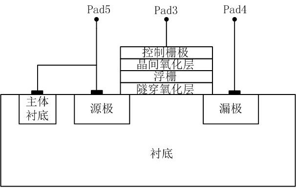
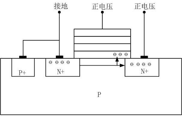
[0030] A test structure for dielectric layer defect detection of the present invention will be described in more detail below in conjunction with schematic diagrams, wherein a preferred embodiment of the present invention is shown, it should be understood that those skilled in the art can modify the present invention described here, and still realize Advantageous effects of the present invention. Therefore, the following description should be understood as the broad knowledge of those skilled in the art, but not as a limitation of the present invention.

[0031] In the interest of clarity, not all features of an actual implementation are described. In the following description, well-known functions and constructions are not described in detail since they would obscure the invention with unnecessary detail. It should be appreciated that in the development of any actual embodiment, numerous implementation details must be worked out to achieve the developer's specific goals, suc...


PUM


Abstract

The invention provides a test structure for dielectric layer defect detection. The test structure comprises a main circuit, a bypass circuit, first to fifth bonding pads and a first switch, wherein the main circuit and the bypass circuit are connected in parallel; the main circuit comprises a to-be-tested capacitor structure; the first bonding pad and the second bonding pad are used for applying avoltage to the main circuit and the bypass circuit; the third bonding pad to the fifth bonding pad are used for editing conduction voltage of the bypass circuit; and the first switch is used for cutting off the circuit of the test structure when the leakage current of the to-be-tested capacitor structure exceeds a preset value. According to the invention, the external voltages of the third pad, the fourth pad and the fifth pad are changed to edit the conduction voltage of the bypass circuit, so that the defect detection items with different electric leakage threshold requirements can share one test structure, the number of the test structures is reduced, the area of a chip scribing channel occupied by the test structure for dielectric layer defect detection can be reduced, and the flexibility of the test structure during testing is improved.

Description

technical field [0001] The invention relates to the technical field of semiconductor manufacturing, in particular to a test structure for detecting dielectric layer defects. Background technique [0002] As a very important structure in the reliability evaluation of semiconductor integrated circuits, the capacitor structure can be used for gate oxide dielectric layers, metal-insulator-metal (MIM) dielectric layers and metal oxide dielectric layers of metal-oxide semiconductor field effect transistors (MOSFETs). - Reliability assessment of oxide-metal (MOM) dielectric layers. [0003] When evaluating the reliability of the capacitor structure, the selection of the leakage threshold is very important. If the leakage threshold is too small, the weak point inside the capacitor will not generate enough leakage, and the location of the weak point of the capacitor structure will not be able to be located in the subsequent failure analysis. ; If the leakage threshold is too large, ...

Claims


Application Information

Patent Timeline
Patent Type & Authority Patents(China)
IPC IPC(8): H01L23/544G01R31/26G01R31/52
CPCG01R31/2639G01R31/52H01L22/32H01L22/34
Inventor 周山王丽雅俞佩佩
Owner 晶芯成(北京)科技有限公司
Features
  • R&D
  • Intellectual Property
  • Life Sciences
  • Materials
  • Tech Scout
  • Unparalleled Data Quality
  • Higher Quality Content
  • 60% Fewer Hallucinations
Learn More