Wear leveling method and device for Nand Flash

A wear leveling, physical block technology, applied in the input/output process of data processing, instruments, electrical digital data processing, etc. Logical page randomness request cannot be done, etc.

Inactive Publication Date: 2020-11-20
SHENZHEN SANDIYIXIN ELECTRONICS CO LTD
View PDF4 Cites 7 Cited by
  • Summary
  • Abstract
  • Description
  • Claims
  • Application Information

AI Technical Summary

Problems solved by technology

[0007] In view of the above-mentioned deficiencies in the prior art, the purpose of the present invention is to provide a wear leveling method and device for Nand Flash, aiming to solve the problem that the effect of the wear leveling algorithm in the prior art is greatly affected by random factors. I don't know the situation of each block being erased, and at the same time, the randomness request for the logical page cannot be completely equal, so the number of erasures of each block cannot reach an equal probability distribution, and a good wear leveling effect cannot be achieved. technical issues

Method used


Image

  • Wear leveling method and device for Nand Flash
  • Wear leveling method and device for Nand Flash

Examples


Embodiment Construction

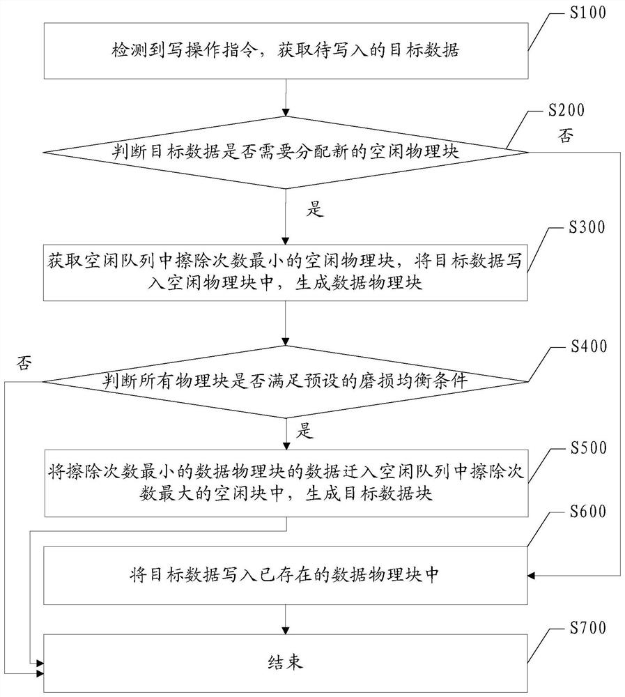
[0036] In order to make the object, technical solution and effect of the present invention more clear and definite, the present invention will be further described in detail below. It should be understood that the specific embodiments described here are only used to explain the present invention, not to limit the present invention. Embodiments of the present invention will be described below in conjunction with the accompanying drawings.

[0037] An embodiment of the present invention provides a wear leveling method for Nand Flash. see figure 1 , figure 1 It is a flowchart of a preferred embodiment of a wear leveling method for Nand Flash in the present invention. Such as figure 1 As shown, it includes the steps:

[0038] Step S100, detecting a write operation instruction, and obtaining target data to be written;

[0039] Step S200, judging whether the target data needs to allocate a new free physical block, if yes, execute step S300, if not, execute step S600;

[0040]...


PUM


Abstract

The invention discloses a wear leveling method and device for Nand Flash, and the method comprises the steps: detecting a writing operation instruction, and obtaining to-be-written target data; judging whether the target data needs to be allocated with a new idle physical block or not; if a new idle physical block needs to be allocated, obtaining the idle physical block with the smallest erasure frequency in the idle queue, writing the target data into the idle physical block, and generating a data physical block; judging whether all the physical blocks meet a preset wear leveling condition ornot; if the preset wear leveling condition is met, migrating the data of the data physical block with the minimum erasure frequency into the idle block with the maximum erasure frequency in the idlequeue to generate a target data block; and repeating the operation until all the physical blocks meet the preset wear leveling condition. According to the embodiment of the invention, the service lifeof the flash memory can be maximized, the influence of data randomness on the service life of the flash memory is solved, and the erasure frequency of each physical block is recorded under the condition of not consuming a large amount of memory resources.

Description

technical field [0001] The invention relates to the technical field of semiconductor devices, in particular to a wear leveling method and device for Nand Flash. Background technique [0002] Nand Flash memory is a kind of flash memory. It adopts nonlinear macro-cell mode inside, which provides a cheap and effective solution for the realization of solid-state large-capacity memory. Nand flash memory has the advantages of large capacity and fast rewriting speed, and is suitable for storing large amounts of data, so it has been more and more widely used in the industry. [0003] Since Nand flash has no rewriting mechanism, after a block is full of data, the data in the block needs to be erased before new data can be written. When the data is updated, rewrite the new data, mark the original data as invalid, and enter the state to be erased. The physical characteristics of solid-state drives determine that their rewritable times are limited. In order to improve the service lif...

Claims


Application Information

Patent Timeline
Patent Type & Authority Applications(China)
IPC IPC(8): G06F3/06
CPCG06F3/0614G06F3/064G06F3/0647G06F3/0652G06F3/0679
Inventor 曾庆聪张如宏胡来胜
Owner SHENZHEN SANDIYIXIN ELECTRONICS CO LTD
Why Eureka
Try Eureka