

Optical waveguide preparation method and optical waveguide
A technology of optical waveguide and photoresist, which is applied in the direction of light guide, optics, optical components, etc., can solve the problems that gratings affect the appearance and use effect, and achieve the effect of improving appearance, use effect and high reliability
- Summary
- Abstract
- Description
- Claims
- Application Information
AI Technical Summary
Problems solved by technology
Method used
Image

Examples
Embodiment Construction
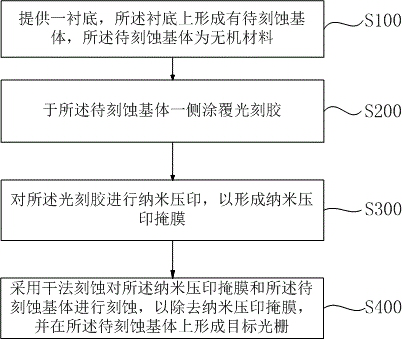
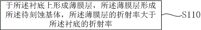
[0031] The following will clearly and completely describe the technical solutions in the embodiments of the present invention with reference to the accompanying drawings in the embodiments of the present invention. Obviously, the described embodiments are only part of the embodiments of the present invention, not all of them. Based on the embodiments of the present invention, all other embodiments obtained by persons of ordinary skill in the art without creative efforts fall within the protection scope of the present invention.
[0032] It should be noted that if there are directional indications (such as up, down, left, right, front, back...) in the embodiment of the present invention, the directional indications are only used to explain how to move in a certain posture (as shown in the accompanying drawings). If the specific posture changes, the directional indication will also change accordingly.
[0033] In addition, if there are descriptions involving "first", "second" an...
PUM
 Abstract
Description
Claims
Application Information