

A kind of anti-radiation reinforced SOI device based on neutron irradiation and its preparation method
A radiation-resistant hardening and device technology, which is applied in semiconductor/solid-state device manufacturing, electrical solid-state devices, semiconductor/solid-state device components, etc., can solve the problem of difficult control of SiGe junction depth, increase device active area area, and lead-out effect To achieve the effect of restoring carrier lifetime and mobility, saving process cost, and reducing parasitic bipolar amplification effect
Active Publication Date: 2022-05-31
XIAMEN UNIV OF TECH
View PDF6 Cites 0 Cited by
- Summary
- Abstract
- Description
- Claims
- Application Information
AI Technical Summary
Problems solved by technology
This method also requires the introduction of additional Ge elements, and the junction depth of the SiGe junction is difficult to control
3. Additional lead-out methods, such as H gate, T gate, ring gate, etc. These methods increase the area of the active area of the device, and for large-width devices, the body lead-out resistance becomes larger, and the body lead-out effect is not good
Method used
View moreImage
Smart ImageViewing Examples

Examples
preparation example Construction
[0045] Or use chemical vapor deposition to grow a single crystal of silicon, so that the silicon layer extends outward to the desired
[0046] So that the surface conduction channel restores a good carrier mobility.
[0055] 6. Laser annealing is performed on the surface of the silicon layer of the device by means of laser annealing. Excimer CW KrF laser
[0058] The present invention can form any
Embodiment 1
[0064] step 4, the device substrate after bonding is processed, so that the surface layer of the silicon layer is restored to a single crystal state;
Embodiment 2
[0067] On the basis of Example 1, an oxide layer is formed on the surface of the device substrate using a thermal oxidation method.
Login to View More PUM
 Abstract
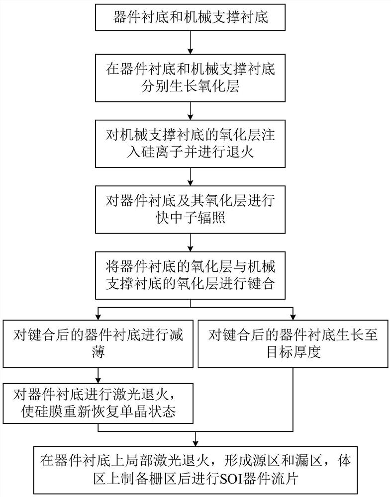
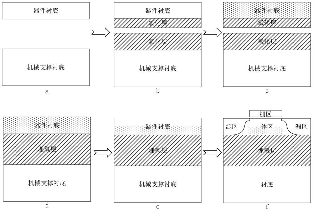
The present invention is an anti-radiation reinforced SOI device based on neutron irradiation and its preparation method. The device includes a substrate, a buried oxide layer and a body region formed sequentially from bottom to top, which are arranged on the same layer as the body region and are isolated from each other. The source region and the drain region, and the gate region arranged on the body region; there are deep level traps introduced by fast neutron irradiation in the body region. The preparation method includes: step 1, growing an oxide layer on the device substrate and a mechanical support substrate respectively; step 2, performing fast neutron irradiation on the oxide layer of the device substrate, so that the silicon layer of the device substrate is formed Deep level trap; step 3, bonding the oxide layer of the mechanical support substrate and the oxide layer of the device substrate after fast neutron irradiation to form an integral buried oxide layer; step 4, bonding the bonded device substrate The substrate is treated to restore the surface of the silicon layer to the single crystal state; step 5, the device tape-out is carried out on the device substrate whose surface layer of the silicon layer has recovered the single crystal state, and the device is prepared.
Description
A kind of radiation-resistant SOI device based on neutron irradiation and preparation method thereof technical field The present invention relates to the field of semiconductor material and device preparation, specifically a kind of anti-radiation reinforcement based on neutron irradiation SOI device and preparation method thereof. Background technique SOI (Silicon-on-Insulator) technology refers to the formation of a single crystal semiconductor with a certain thickness on the insulating layer The material preparation technology of bulk silicon thin film layer and the process technology of manufacturing semiconductor device on the thin film layer. SOI technology can achieve Full dielectric isolation of the device, with no latch-up, high speed, low power consumption, high integration compared to bulk silicon technology with PN junction isolation It has the advantages of high temperature, high temperature resistance, and strong radiation resistance, and is widely use...
Claims
Login to View More Application Information
Patent Timeline
 Patent Type & AuthorityPatents(China)
IPC IPC(8): H01L23/552H01L29/78H01L21/263H01L21/336
CPCH01L23/552H01L29/78H01L21/263H01L29/66477Y02P70/50
Inventor黄辉祥毕大炜韦素芬潘金艳林海军陈铖颖
OwnerXIAMEN UNIV OF TECH