Anti-radiation reinforced SOI device based on neutron irradiation and preparation method thereof

An anti-radiation hardening and device technology, which is used in semiconductor/solid-state device manufacturing, electrical solid-state devices, semiconductor/solid-state device components, etc. It can restore the carrier lifetime and mobility, avoid interface incompatibility, and save process costs.

Active Publication Date: 2020-11-24
XIAMEN UNIV OF TECH
View PDF6 Cites 1 Cited by
  • Summary
  • Abstract
  • Description
  • Claims
  • Application Information

AI Technical Summary

Problems solved by technology

This method also requires the introduction of additional Ge elements, and the junction depth of the SiGe junction is difficult to control
3. Additional lead-out methods, such as H gate, T gate, ring gate, etc. These methods increase the area of ​​the active area of ​​the device, and for large-width devices, the body lead-out resistance becomes larger, and the body lead-out effect is not good

Method used


Image

  • Anti-radiation reinforced SOI device based on neutron irradiation and preparation method thereof
  • Anti-radiation reinforced SOI device based on neutron irradiation and preparation method thereof
  • Anti-radiation reinforced SOI device based on neutron irradiation and preparation method thereof

Examples


preparation example Construction

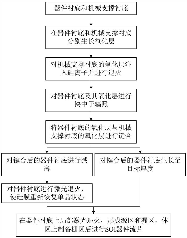
[0038] On the basis of the original preparation method of anti-total dose radiation SOI material, the present invention proposes a new method of introducing deep energy level traps in the body region by using the effect of neutron irradiation, effectively reducing the parasitic bipolar of partially depleted SOI devices Magnification effect. Such as figure 1 As shown, it includes the following steps:

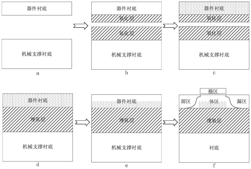
[0039]1. Prepare two monocrystalline silicon substrates, one of which is used as a mechanical support substrate, and the other monocrystalline silicon substrate is used as a device substrate for preparing devices;

[0040] 2. The surface of the device substrate is thermally oxidized to form an oxide layer of the silicon dioxide layer; the surface of the mechanical support substrate is first thermally oxidized to form an oxide layer, and then the CVD method is used to form an oxide layer with a target thickness;

[0041] 3. Si ions are implanted into the oxide layer of the mecha...

Embodiment 1

[0060] A method for preparing an anti-radiation reinforced SOI device based on neutron irradiation, comprising the following steps,

[0061] Step 1, growing an oxide layer on the device substrate and the mechanical support substrate respectively;

[0062] Step 2, irradiating the oxide layer of the device substrate with fast neutrons, so that deep energy level traps are formed in the silicon layer of the device substrate;

[0063] Step 3, bonding the oxide layer of the mechanical support substrate and the oxide layer of the device substrate after fast neutron irradiation to form an integral buried oxide layer;

[0064] Step 4, processing the bonded device substrate so that the surface layer of the silicon layer can be restored to a single crystal state;

[0065] Step 5: Tape out the device on the device substrate whose surface layer of the silicon layer has returned to a single crystal state, and prepare a radiation-resistant and strengthened SOI device based on neutron irradi...

Embodiment 2

[0067] On the basis of Embodiment 1, an oxide layer is formed on the surface of the device substrate by thermal oxidation.


PUM


Abstract

The invention discloses an anti-radiation reinforced SOI device based on neutron irradiation and a preparation method thereof. The device comprises a substrate, a buried oxide layer, a body region, asource region, a drain region and a gate region arranged on the body region, wherein the substrate, the buried oxide layer and the body region are sequentially formed from bottom to top; the source region and the drain region are arranged on the same layer as the body region and isolated from each other; and a deep energy level trap introduced through fast neutron irradiation is arranged in the body region. The preparation method comprises the following steps: step 1, respectively growing oxide layers on the device substrate and a mechanical support substrate; 2, performing fast neutron irradiation on the oxide layer of the device substrate to form the deep energy level trap in a silicon layer of the device substrate; 3, bonding the oxide layer of the mechanical support substrate and theoxide layer of the device substrate subjected to fast neutron irradiation to form the integral buried oxide layer; step 4, processing the bonded device substrate to enable the surface layer of the silicon layer to recover the single crystal state again; and step 5, carrying out device tape-out on the device substrate of which the surface layer of the silicon layer is recovered to the single crystal state to prepare the device.

Description

technical field [0001] The invention relates to the field of semiconductor materials and device preparation, in particular to a radiation-resistant and reinforced SOI device based on neutron irradiation and a preparation method thereof. Background technique [0002] SOI (Silicon-on-Insulator) technology refers to the material preparation technology of forming a single crystal semiconductor silicon thin film layer with a certain thickness on the insulating layer and the process technology of manufacturing semiconductor devices on the thin film layer. SOI technology can realize full dielectric isolation of devices. Compared with bulk silicon technology isolated by PN junction, it has the advantages of no latch, high speed, low power consumption, high integration, high temperature resistance, and strong radiation resistance. It is widely used in high-speed, low power consumption, and radiation-resistant circuits. [0003] Since the SOI process MOS device is formed above the bu...

Claims


Application Information

Patent Timeline
Patent Type & Authority Applications(China)
IPC IPC(8): H01L23/552H01L29/78H01L21/263H01L21/336
CPCH01L23/552H01L29/78H01L21/263H01L29/66477Y02P70/50
Inventor 黄辉祥毕大炜韦素芬潘金艳林海军陈铖颖
Owner XIAMEN UNIV OF TECH
Why Eureka
Try Eureka