Wafer clamping device for semiconductor packaging

A technology of semiconductors and clips, which is applied in the manufacture of semiconductor/solid-state devices, electrical components, circuits, etc., can solve the problems of metal pin clamping is not firm, semiconductor integrated circuit damage, metal pins are easy to break, etc., to avoid metal pins The effect of pin breakage, breakage prevention, and excessive clamping force prevention

Inactive Publication Date: 2020-11-27
菏泽景月装饰有限公司
View PDF0 Cites 1 Cited by
  • Summary
  • Abstract
  • Description
  • Claims
  • Application Information

AI Technical Summary

Problems solved by technology

[0002] Dual-in-line packaging is one of the packaging methods of semiconductor integrated circuits. The shape of the integrated circuit is rectangular, and there are two rows of parallel metal pins on both sides. The integrated circuit clamps the metal pins to ensure normal packaging work, but because the clipper clamps the metal pins in the process, in order to improve the firmness of the clamping, the clamping force is too strong, thus The extrusion force between the metal pin and the clip is too large, and the metal pin is relatively small, causing the metal pin to break easily inside the clip, and it is difficult to take it out from the gap of the clip, resulting in damage to the semiconductor integrated circuit , and cause the clamper to not firmly clamp the metal pin of the next semiconductor integrated circuit

Method used


Image

  • Wafer clamping device for semiconductor packaging
  • Wafer clamping device for semiconductor packaging
  • Wafer clamping device for semiconductor packaging

Examples


Embodiment 1

[0022] as attached figure 1 to attach Figure 5 Shown:

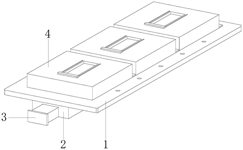
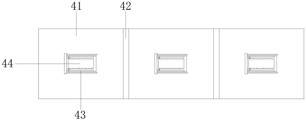
[0023] The present invention is a clipper for semiconductor packaging, its structure includes a mounting plate 1, a slide rail 2, a drive rod 3, and a clamping mechanism 4, the bottom of the mounting plate 1 is welded with a slide rail 2, and the drive rod 3 adopts clearance fit Through the inside of the slide rail 2, a clamping mechanism 4 is welded on the upper surface of the mounting plate 1, and the clamping mechanism 4 includes a fixing groove 41, a slant plate 42, a side clamping mechanism 43, and an inner support mechanism 44. The fixing groove The bottom of 41 is fixedly welded on the upper surface of the mounting plate 1, and the inclined plate 42 is arranged at the lower end of the right side of the fixing groove 41, and the side clamping mechanism 43 is installed inside the fixing groove 41, and the side clamping mechanism 43 is located outside the inner support mechanism 44, so There are three fixing groove...

Embodiment 2

[0030] as attached Figure 6 to attach Figure 7 Shown:

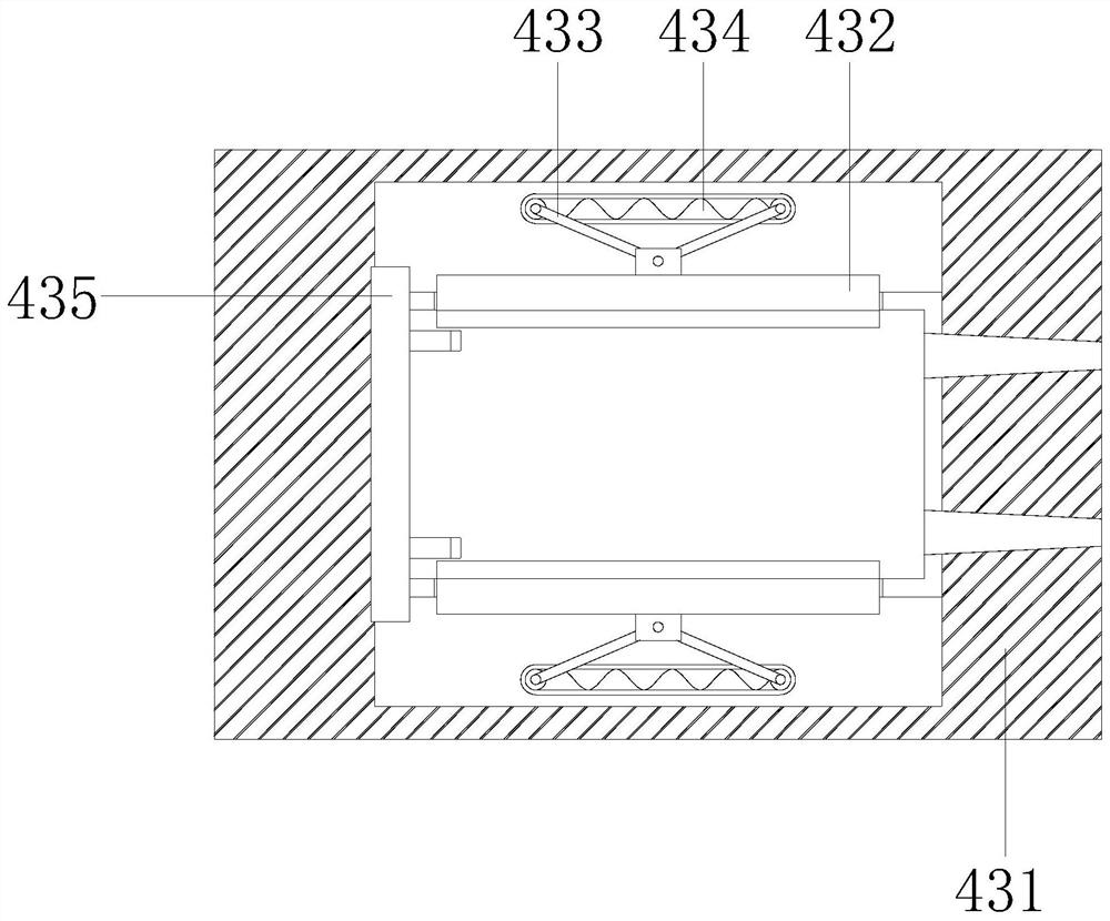
[0031] Wherein, the inner support mechanism 44 includes a support plate 44a, an extrusion plate 44b, and an engaging mechanism 44c. The lower end of the support plate 44a is fixedly installed on the inner bottom surface of the fixing seat 431, and the upper end surface of the support plate 44a is embedded with an extrusion plate. 44b, and the extrusion plate 44b is connected to the inner middle end of the engaging mechanism 44c, the engaging mechanism 44c is arranged on the outside of the support plate 44a, the cross section of the support plate 44a is rectangular, and matches the shape of the integrated circuit, It is beneficial to place the bottom surface of the integrated circuit on the upper surface of the support plate 44a. There are two engaging mechanisms 44c, which are respectively arranged on the front and rear surfaces of the support plate 44a, which is beneficial to the two rows of parallel metal pins of the...


PUM


Abstract

The invention discloses a wafer clamping device for semiconductor packaging. The clamping device structurally comprises a mounting plate, a sliding rail, a driving rod and a clamping mechanism. A slide rail is welded at the bottom of the mounting plate. The driving rod penetrates through the interior of the sliding rail in a clearance fit manner. The metal pins are attached and fixed through the magnetic adsorption force of the magnetic plate. Therefore, the clamping force is prevented from being too large. Excessive extrusion force on the metal pin is avoided. The sliding rod drives the supporting rod and the scraping plate to stably slide in a clamping gap groove in the fixed seat. Foreign matters in the gap groove are scraped. The metal pins of the semiconductor integrated circuit are just clamped and limited with the outer side surfaces of the clamping sheets. Meanwhile, the bottom surface of the semiconductor integrated circuit extrudes the extrusion plate downwards, so that the extrusion plate extrudes the interior of the air pressure chamber, the air pressure in the air bag film is increased to bulge, the bulged air bag film pushes against the metal pin to buffer the metal pin, and the metal pin is prevented from being broken due to overlarge clamping force.

Description

technical field [0001] The invention relates to the field of semiconductors, and more specifically, to a clipper for semiconductor packaging. Background technique [0002] Dual-in-line packaging is one of the packaging methods of semiconductor integrated circuits. The shape of the integrated circuit is rectangular, and there are two rows of parallel metal pins on both sides. The integrated circuit clamps the metal pins to ensure normal packaging work, but because the clipper clamps the metal pins in the process, in order to improve the firmness of the clamping, the clamping force is too strong, thus The extrusion force between the metal pin and the clip is too large, and the metal pin is relatively small, causing the metal pin to break easily inside the clip, and it is difficult to take it out from the gap of the clip, resulting in damage to the semiconductor integrated circuit , and cause the clipper to not firmly clamp the metal pin of the next semiconductor integrated ci...

Claims


Application Information

Patent Timeline
Patent Type & Authority Applications(China)
IPC IPC(8): H01L21/683
CPCH01L21/6838
Inventor 傅梅英
Owner 菏泽景月装饰有限公司
Why Eureka
Try Eureka