Display panel, manufacturing method thereof and display device

A technology for display panels and substrate substrates, which is applied in semiconductor/solid-state device manufacturing, diodes, semiconductor devices, etc., and can solve problems such as poor display effects of display devices

Pending Publication Date: 2020-11-27
BOE TECH GRP CO LTD
View PDF10 Cites 3 Cited by
  • Summary
  • Abstract
  • Description
  • Claims
  • Application Information

AI Technical Summary

Problems solved by technology

[0005] The present application provides a display panel, its manufacturing method, and a display device, which can solve the problem of poor display effect of the display device in the related art

Method used


Image

  • Display panel, manufacturing method thereof and display device
  • Display panel, manufacturing method thereof and display device
  • Display panel, manufacturing method thereof and display device

Examples


Embodiment Construction

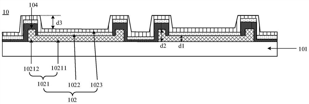
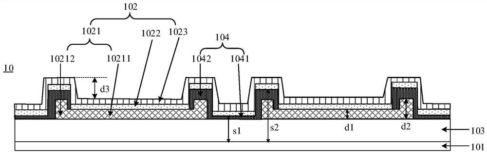
[0057] In order to make the purpose, technical solution and advantages of the present application clearer, the implementation manners of the present application will be further described in detail below in conjunction with the accompanying drawings.

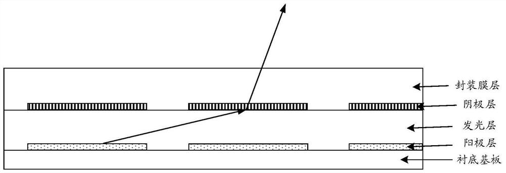
[0058] Silicon-based OLED display panels are widely used in virtual reality (virtual reality, VR) equipment, augmented reality (augmented reality) equipment, camera viewfinders or sights due to their advantages of ultra-high pixel density (pixels per inch, PPI). .

[0059] However, due to the small size of the sub-pixels in the silicon-based OLED display panel, the fabrication accuracy of the light-emitting layer of the sub-pixel 102 is low by using a mask. Therefore, under normal circumstances, the display panel can be prepared by adopting the scheme of white light OLED and color filter layer. That is, the light emitted by each sub-pixel in the display panel is white light, and the white light passes through the color filter la...


PUM

PropertyMeasurementUnit
thicknessaaaaaaaaaa
thicknessaaaaaaaaaa

Abstract

The invention discloses a display panel, a manufacturing method thereof and a display device, and relates to the technical field of display. The thickness of the second part of the first electrode ofthe sub-pixel in the display panel can be relatively large; the light-emitting film layer can be blocked; light emitted by part of the film layer located above the first part of the first electrode istransmitted to the area where the adjacent sub-pixel is located, light emitted by the light-emitting film layer in the sub-pixel is prevented from being emitted out of the second electrode of the adjacent sub-pixel, then crosstalk of light of multiple sub-pixels is prevented, and the display effect of the display device is good.

Description

technical field [0001] The present application relates to the field of display technology, in particular to a display panel, a manufacturing method thereof, and a display device. Background technique [0002] An organic light-emitting diode (OLED) display panel has been widely used due to its advantages of self-illumination, low driving voltage, and fast response speed. [0003] In related technologies, an OLED display panel may include: a plurality of OLED sub-pixels of different colors. Each OLED sub-pixel includes: an anode layer, a cathode layer, and a light emitting layer located between the anode layer and the cathode layer. Wherein, the light-emitting layer can emit light under the drive of the anode layer and the cathode layer. [0004] However, due to the short distance between multiple OLED sub-pixels, the light emitted by the light-emitting layer in the OLED sub-pixel may be emitted from the cathode layer of the OLED sub-pixel adjacent to the OLED sub-pixel, and...

Claims


Application Information

Patent Timeline
Patent Type & Authority Applications(China)
IPC IPC(8): H01L51/52H01L51/56H01L27/32
CPCH10K59/38H10K59/12H10K50/813H10K50/86H10K71/00H10K2102/351H10K59/122H10K59/1201
Inventor 李晓虎闫华杰王路焦志强
Owner BOE TECH GRP CO LTD
Why Eureka
Try Eureka