Optical transmission prism, optical output device, and optical input device

An optical transmission and prism technology, applied in the field of optical communication, can solve the problem that the optical waveguide chip cannot integrate the light source, and achieve the effect of reducing the volume and reducing the cost.

Inactive Publication Date: 2020-12-08
GUANGXUN SCI & TECH WUHAN
View PDF2 Cites 0 Cited by
  • Summary
  • Abstract
  • Description
  • Claims
  • Application Information

AI Technical Summary

Problems solved by technology

However, optical waveguide chips cannot integrate light sources, so an exter

Method used


Image

  • Optical transmission prism, optical output device, and optical input device
  • Optical transmission prism, optical output device, and optical input device
  • Optical transmission prism, optical output device, and optical input device

Examples


Embodiment Construction

[0034] In order to make the technical solutions and advantages of the embodiments of the present invention clearer, the technical solutions in the embodiments of the present invention will be clearly and completely described below in conjunction with the drawings in the embodiments of the present invention. Obviously, the described embodiments are the Some, but not all, embodiments are invented.

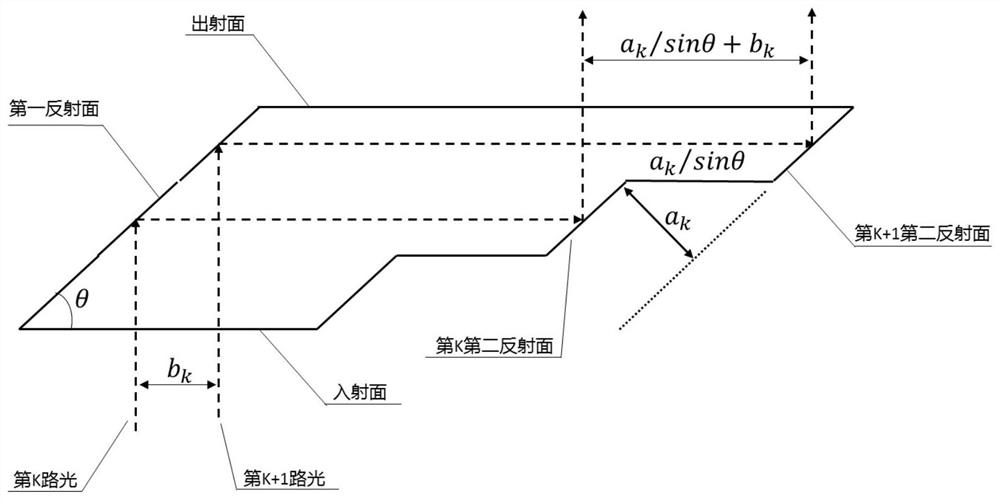
[0035] Generally, the coupling between multi-channel laser or detector and optical waveguide, the input waveguide spacing and the laser or detector spacing are equal, only in this way can the light of laser or detector be input into the optical waveguide one by one. Generally, the width of the laser chip is about 250um, and the width of the auxiliary package structure such as the heat sink is about 1mm. Therefore, the distance between the optical waveguide chip and the multi-channel laser is often more than 1mm. With the existing optical waveguide technology, whether it is a silicon ...


PUM


Abstract

The invention relates to an optical transmission prism, an optical output device and an optical input device. The optical transmission prism comprises an incident plane; a first reflecting surface, wherein an included angle theta is formed between the first reflecting surface and the incident surface; at least two second reflecting surfaces parallel to the first reflecting surface, wherein the distance between the kth reflecting surface and the first reflecting surface in the second reflecting surfaces is smaller than the distance between the (k+1) th reflecting surface and the first reflecting surface, and k is a positive integer; and an emergent surface parallel to the incident surface and intersecting with the edge of the first reflecting surface and the edges of the second reflecting surfaces, so that the distance between the parallel incident light is changed through the first reflecting surface and the plurality of second reflecting surfaces.

Description

technical field [0001] The invention relates to the technical field of optical communication, in particular to an optical transmission prism, an optical output device, and an optical input device. Background technique [0002] Optoelectronic devices are the core components of optical fiber communication. With the development of optoelectronic devices towards high speed, high packaging density, low cost, and low power consumption, integrated packaging technology is playing an increasingly important role in the packaging of optoelectronic devices. Integrated packaging is to use optical waveguide technology to integrate modulation, multiplexing / demultiplexing and other functions on the optical waveguide chip, which can increase the packaging density and increase the reliability of the optical path. However, optical waveguide chips cannot integrate light sources, so an external light source is required to couple light into the optical waveguide chip. In the process of coupling...

Claims


Application Information

Patent Timeline
IPC IPC(8): G02B6/42G02B6/43
CPCG02B6/4214G02B6/43
Inventor 朱虎周日凯付永安杜书剑郭燕玲刘弘扬
Owner GUANGXUN SCI & TECH WUHAN
Why Eureka
Try Eureka