Mini LED device easy to identify and module

A technology of devices and modules, which is applied in the field of Mini LED devices and modules, can solve problems such as the decline in yield rate, the inability to judge whether the placement is correct through the front, and achieve the effect of easy identification of the direction

Pending Publication Date: 2021-01-01
APT ELECTRONICS
View PDF0 Cites 0 Cited by
  • Summary
  • Abstract
  • Description
  • Claims
  • Application Information

AI Technical Summary

Problems solved by technology

Since the front side of the Mini LED device cannot be marked, it is impossible to judge whether the placement is correct through the front side during the placement process, which leads to the problem that the error cannot be detected in the previous process, resulting in a decrease in yield

Method used


Image

  • Mini LED device easy to identify and module
  • Mini LED device easy to identify and module
  • Mini LED device easy to identify and module

Examples


Embodiment 1

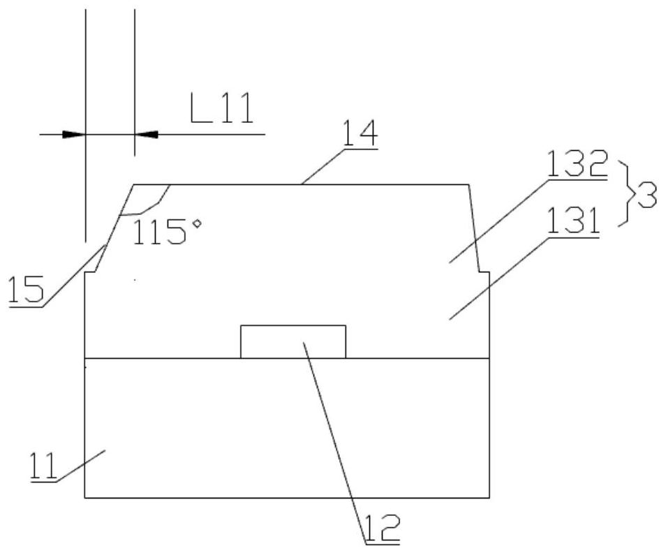
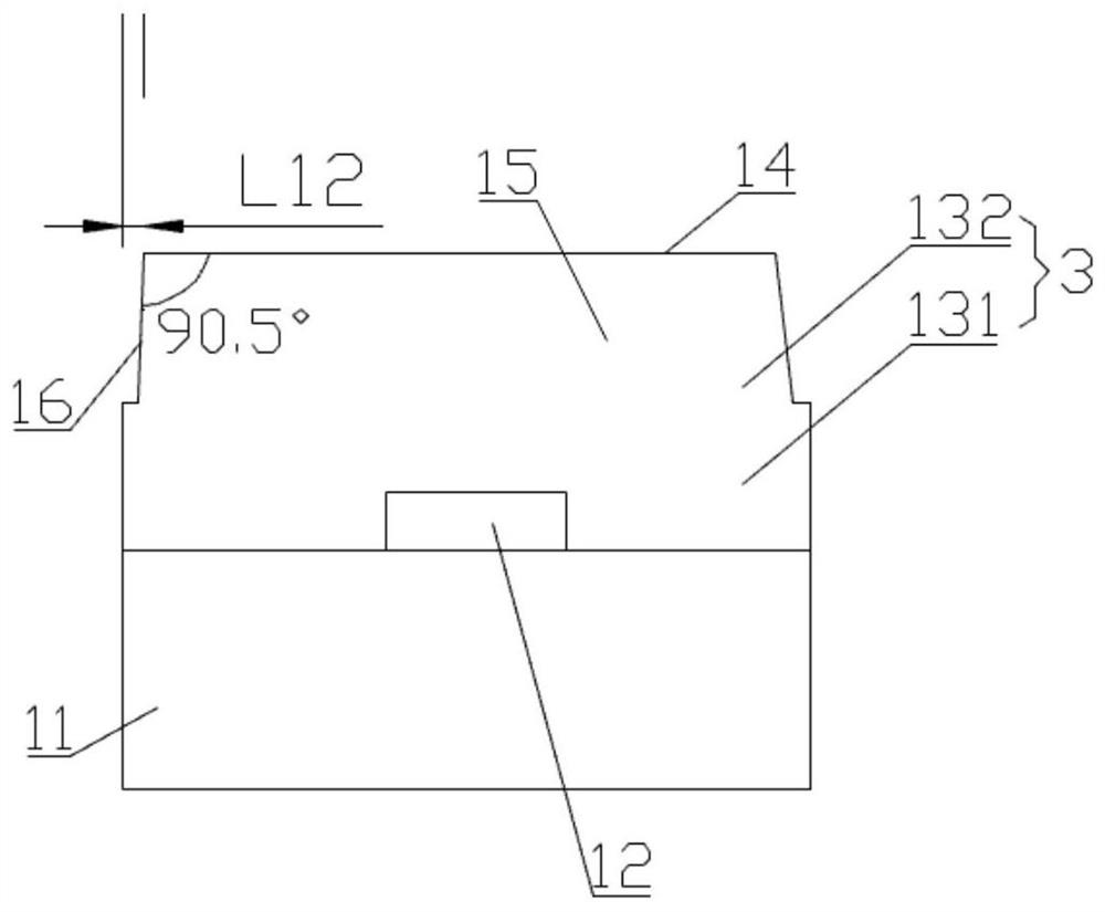
[0031] This embodiment discloses an easily identifiable Mini LED device 1, such as figure 1 and figure 2 As shown, it includes: a substrate 11, a pixel chip 12 and a protective layer 13; the pixel chip 12 is arranged on the substrate 11; wherein, the pixel chip 12 includes a red chip 121 displaying red, a green chip 122 displaying green and a blue chip 122. The blue chip 123; the protection layer 13 includes a first protection layer 131 and a second protection layer 132 in the shape of a quadrangular pyramid; the first protection layer 131 is arranged above the substrate 11 and covers the outside of the pixel chip 12; The second protective layer 132 is arranged on the top of the first protective layer 131; the upper surface 14 of the second protective layer 132 forms a first angle with the first side 15 of the second protective layer 132, and the upper surface 14 of the second protective layer 132 It forms a second included angle with the second side 16 of the second protect...

Embodiment 2

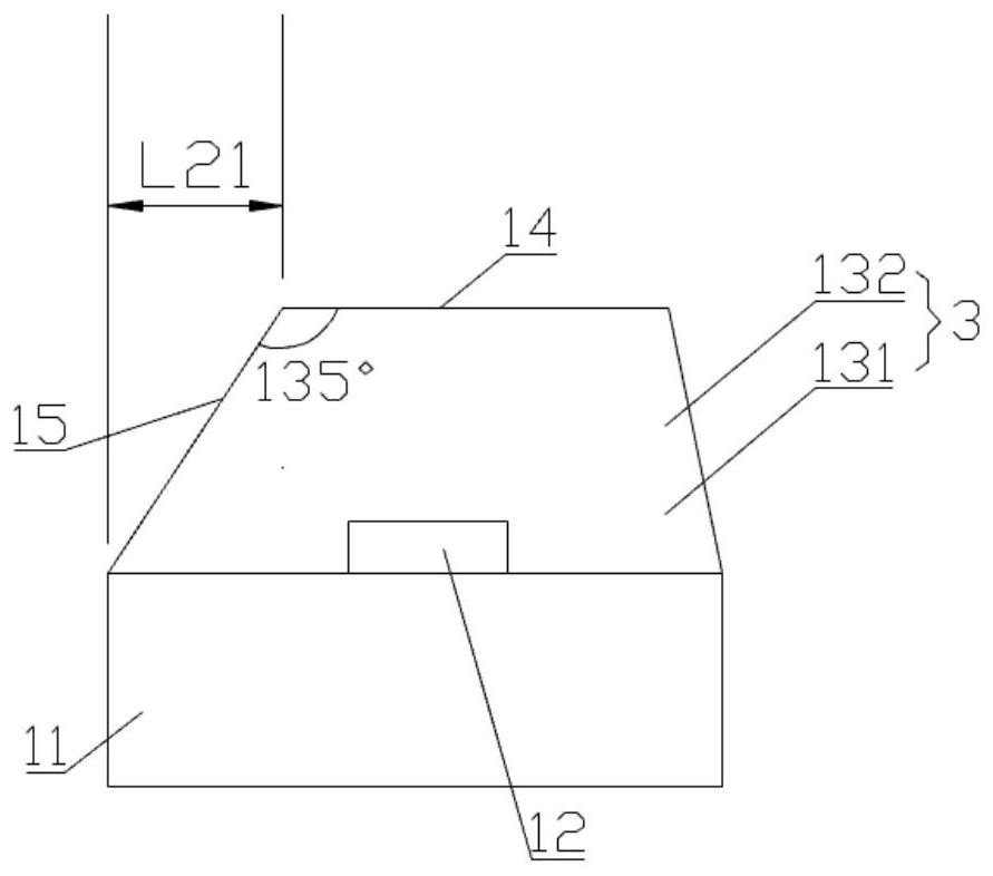
[0037] This embodiment provides another easily identifiable Mini LED device 1, such as image 3 and Figure 4 As shown, the difference between it and Embodiment 1 is that the first included angle is equal to 135°, and the second included angle is equal to 113°, so that L21 and L22 are not equal, so that the front and back of the Mini LED device 1 can be easily identified from the front, The first protection layer 131 is arranged in a rectangular truss shape, and is smoothly connected with the second protection layer 132 . The principle of this embodiment is the same as that of Embodiment 1, and will not be repeated here.

Embodiment 3

[0039] This embodiment provides another easily identifiable Mini LED device 1. The difference between it and Embodiment 1 is that the first included angle is equal to 155°, and the second included angle is equal to 165°. The principle of this embodiment is the same as that of Embodiment 1. The same, and will not repeat them one by one here.


PUM


Abstract

The invention discloses a Mini LED device easy to identify and a module thereof. The Mini LED device comprises a substrate, a pixel chip and a protective layer. The pixel chip is arranged on the substrate; the protective layer comprises a first protective layer and a quadrangular frustum pyramid-shaped second protective layer; the first protective layer is arranged above the substrate and wraps the pixel chip; the second protective layer is arranged at the top of the first protective layer; a first included angle is formed between the upper surface of the second protective layer and the firstside surface of the second protective layer, a second included angle is formed between the upper surface of the second protective layer and the second side surface of the second protective layer, thefirst side surface and the second side surface are two adjacent side surfaces, and the first included angle is not equal to the second included angle; the distances between the edge of the upper surface of the second protective layer and the edges of the two adjacent side faces (namely the connecting positions of the second protective layer and the first protective layer) are unequal, and the MiniLED device can be recognized from the front face through the two unequal distances.

Description

technical field [0001] The invention belongs to the technical field of LED displays, and in particular relates to an easily identifiable Mini LED device and module. Background technique [0002] Micron-sized Mini LED has become a recent research hotspot due to its advantages of high brightness, high contrast, high color saturation, and local dimming. Mini LED is expected to replace LCD and OLED as the next generation of new display technology. Consumers have higher and higher requirements for the resolution and color consistency of LED displays, which put forward higher requirements for traditional LED display devices. Combined with Mini's high-resolution Mini LED devices, due to the relative cost of the process conditions, it is gradually applied in small-pitch display screens in batches. Since Mini LED devices cannot be marked on the front side, it is not possible to judge whether the placement is correct through the front side during the placement process, which leads to...

Claims


Application Information

Patent Timeline
Patent Type & Authority Applications(China)
IPC IPC(8): G09F9/33H01L23/544H01L27/15
CPCG09F9/33H01L23/544H01L27/156
Inventor 万垂铭姚述光曾照明谢超英于智松肖国伟
Owner APT ELECTRONICS
Why Eureka
Try Eureka