Efficient light absorption monocrystalline silicon wafer
A monocrystalline silicon wafer, high-efficiency technology, applied in the direction of photovoltaic modules, photovoltaic power generation, photovoltaic module support structures, etc., can solve the problems of different irradiation angles and low light absorption efficiency, and achieve the effect of convenient adjustment and convenient disassembly
- Summary
- Abstract
- Description
- Claims
- Application Information
AI Technical Summary
Problems solved by technology
Method used
Image

Examples
Embodiment Construction
[0025] The following will clearly and completely describe the technical solutions in the embodiments of the present invention with reference to the accompanying drawings in the embodiments of the present invention. Obviously, the described embodiments are only some, not all, embodiments of the present invention. Based on the embodiments of the present invention, all other embodiments obtained by persons of ordinary skill in the art without making creative efforts belong to the protection scope of the present invention.
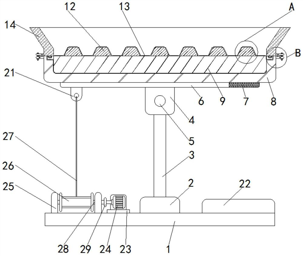
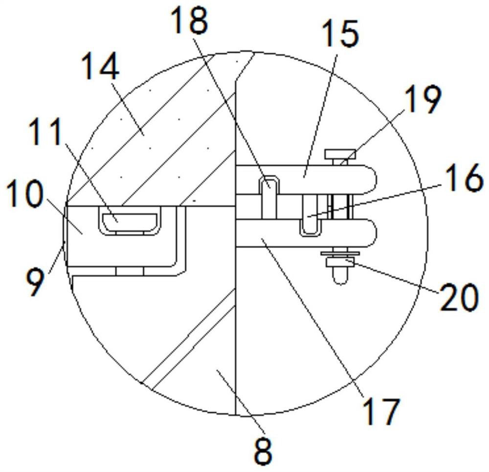
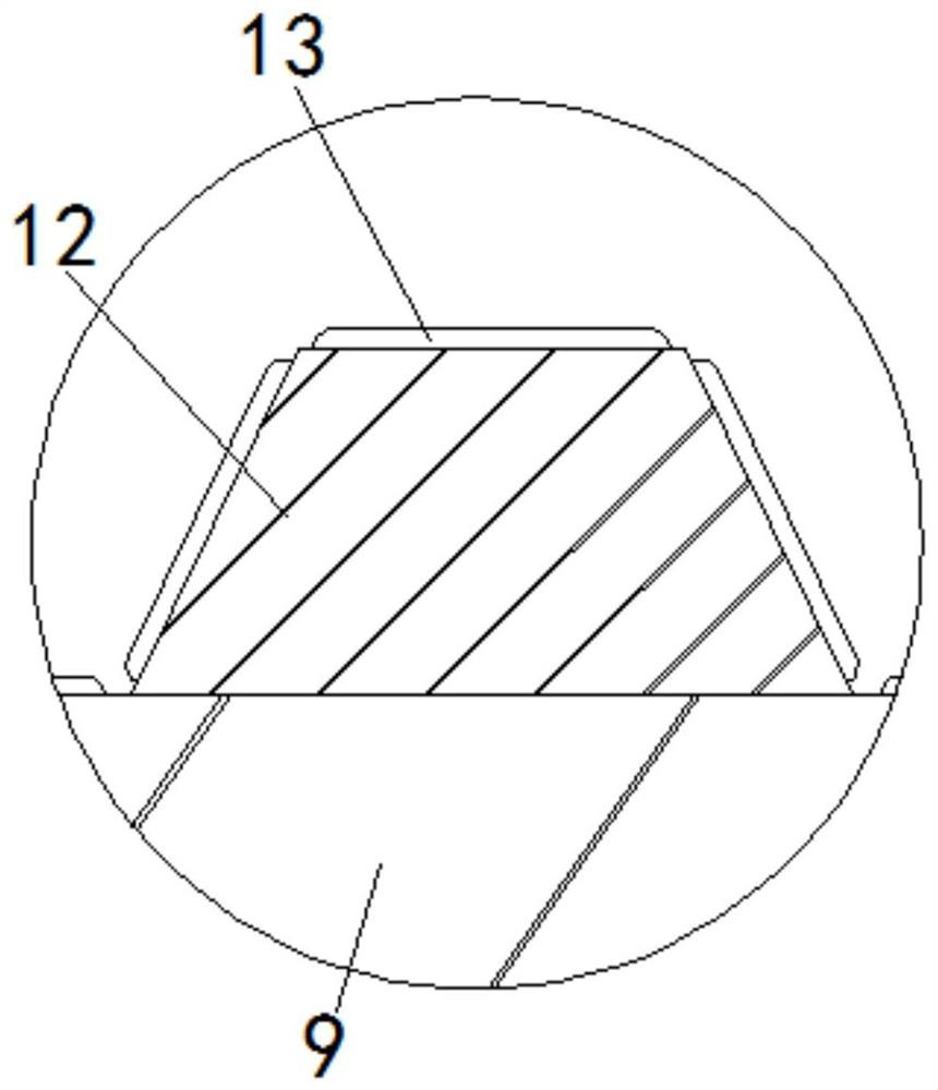
[0026] see Figure 1-4 , the high-efficiency light-absorbing monocrystalline silicon wafer includes a backing plate 1, a strut sleeve 2 is fixedly installed on the top of the backing plate 1, a sponge pad 22 is fixedly installed on the right side of the strut sleeve 2, and a The strut 3 and the strut sleeve 2 are located in the middle of the top surface of the backing plate 1. The inner side of the strut sleeve 2 is provided with an installation socket suitabl...
PUM
 Abstract
Description
Claims
Application Information
 - R&D Engineer
- R&D Manager
- IP Professional
- Industry Leading Data Capabilities
- Powerful AI technology
- Patent DNA Extraction
Browse by: Latest US Patents, China's latest patents, Technical Efficacy Thesaurus, Application Domain, Technology Topic.
© 2024 PatSnap. All rights reserved.Legal|Privacy policy|Modern Slavery Act Transparency Statement|Sitemap