Silicon-based ultra-wide spectrum photon absorber and preparation method thereof

A photon absorption, ultra-broadband technology, applied in the field of nanophotonics

Pending Publication Date: 2021-01-08
苏州斯特科光电科技有限公司
View PDF0 Cites 3 Cited by
  • Summary
  • Abstract
  • Description
  • Claims
  • Application Information

AI Technical Summary

Problems solved by technology

[0004] The invention aims to solve the problem that silicon-based optical and optoelectronic devices in the prior art cannot p

Method used


Image

  • Silicon-based ultra-wide spectrum photon absorber and preparation method thereof
  • Silicon-based ultra-wide spectrum photon absorber and preparation method thereof
  • Silicon-based ultra-wide spectrum photon absorber and preparation method thereof

Examples


Embodiment

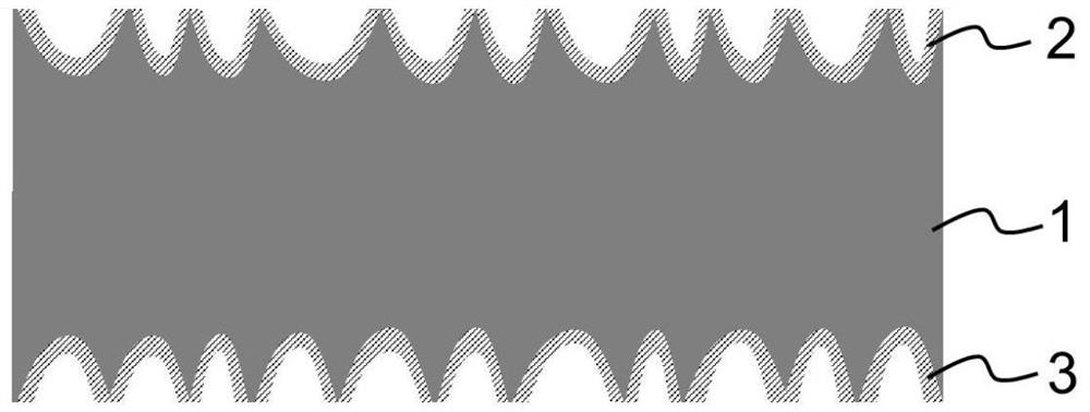
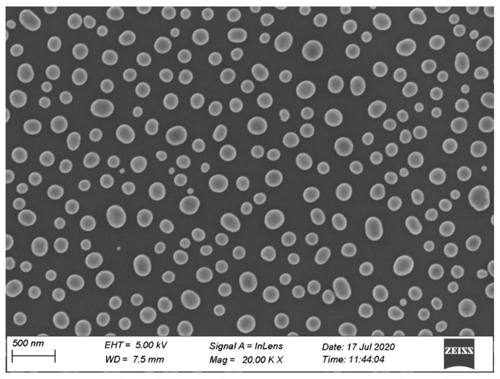
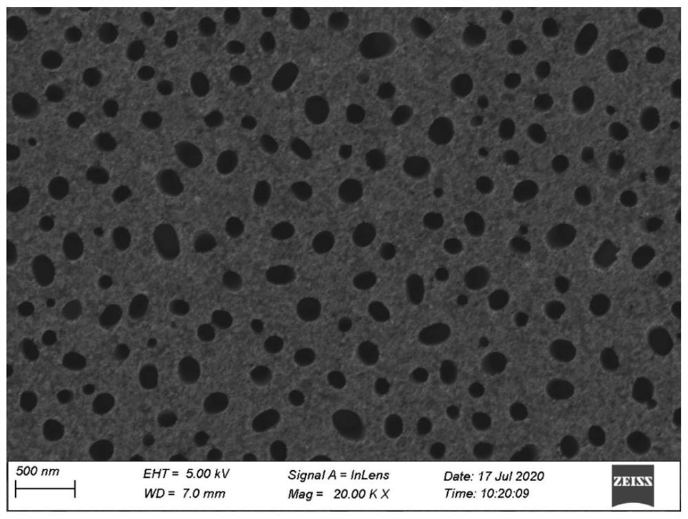
[0041] A silicon-based ultra-broadband photon absorber, such as figure 1 As shown: the photon absorber is a composite layer structure, which sequentially includes the first metal thin film layer 2, the first disordered nanobowl array layer, the silicon substrate 1, and the second disordered nanobowl array layer along the light incident direction , the second metal thin film layer 3; the first disordered nanobowl array layer and the second disordered nanobowl array layer are obtained by etching on a double-sided polished silicon substrate; the first metal thin film layer is obtained by first The disordered nanobowl array layer is obtained by depositing the substrate, and the second metal thin film layer is obtained by depositing the second disordered nanobowl array layer as the substrate: the nanobowl array presents a disordered arrangement, and the diameter and depth are respectively 40-500nm and 50-1000nm randomly distributed within the range.

[0042] Using double-sided pol...


PUM

PropertyMeasurementUnit
Thicknessaaaaaaaaaa

Abstract

The invention belongs to the field of nanophotonics, and provides a silicon-based ultra-wide spectrum photon absorber and a preparation method thereof, and aims to solve the technical problem that inthe prior art, silicon-based optical and photoelectric devices cannot achieve efficient absorption in ultraviolet, visible and near-infrared bands. The absorber comprises a first metal film layer, a first disordered nano bowl array layer, a silicon substrate, a second disordered silicon nano bowl array layer and a second metal film layer, a double-sided disordered metal/silicon nano bowl array composite structure can efficiently absorb more than 80% of incident photons within the waveband range of 200-2500nm, is insensitive to the polarization and angle of incident light, and has a wide application prospect in the fields of photoelectric detection and reverse detection, solar cells, photoelectric sensing and the like.

Description

technical field [0001] The invention relates to a photon absorber capable of high-efficiency absorption in the range of ultraviolet-visible-near-infrared bands and a preparation method thereof, in particular to a light field control technology in an ultra-wide band range, and belongs to the field of nanophotonics. Background technique [0002] A perfect broad-spectrum photon absorber is a device that can completely absorb incident light with a wide range of wavelengths or frequencies (that is, without reflection and transmission). Sensing, optical communication and other fields have a very wide range of applications. It usually uses the surface treatment or multi-layer structure of the device to regulate the light field of the incident light, making it localized inside the light-absorbing material layer to significantly enhance the absorption efficiency of the light-absorbing material, while suppressing the overall reflectivity and transmittance of the device. [0003] At p...

Claims


Application Information

Patent Timeline
IPC IPC(8): H01L31/0224H01L31/0232H01L31/0352H01L31/0236H01L31/108H01L31/18B82Y15/00B82Y40/00
CPCB82Y15/00B82Y40/00H01L31/022408H01L31/022466H01L31/02327H01L31/02363H01L31/035281H01L31/1085H01L31/1804Y02E10/547Y02P70/50
Inventor 吴绍龙詹纯
Owner 苏州斯特科光电科技有限公司
Why Eureka
Try Eureka