Chip failure positioning method and clamp

A failure location, chip technology, applied in the direction of electronic circuit testing, measuring devices, instruments, etc., can solve the problems of increasing position deviation, failing to power on the chip, destroying the chip structure layer, etc.

Pending Publication Date: 2021-01-22
SHENZHEN STS MICROELECTRONICS
View PDF1 Cites 2 Cited by
  • Summary
  • Abstract
  • Description
  • Claims
  • Application Information

AI Technical Summary

Problems solved by technology

The movement process of this method increases the possibility of position deviation, and its accuracy cannot be very high
[0007] In addition, the existing laser marking method uses a high-power laser to mark the surface of the chip with a micron-level depth. This method directly destroys the chip structure

Method used


Image

  • Chip failure positioning method and clamp
  • Chip failure positioning method and clamp
  • Chip failure positioning method and clamp

Examples


Embodiment 1

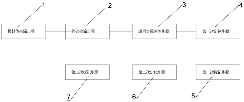
[0066] Such as figure 1 , Figure 8 and Figure 10 As shown, in the transfer step, the side of the chip body 10 facing the lens of the low-light microscope is the front side 101, and the front side 101 of the chip is marked by the imaging marking device, that is, the method for marking the front side 101 of the chip. The specific steps are as follows:

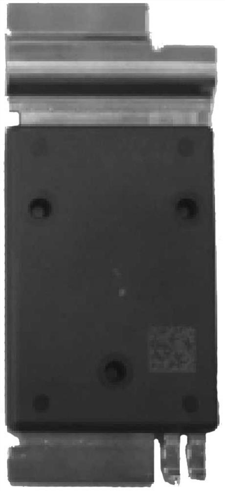
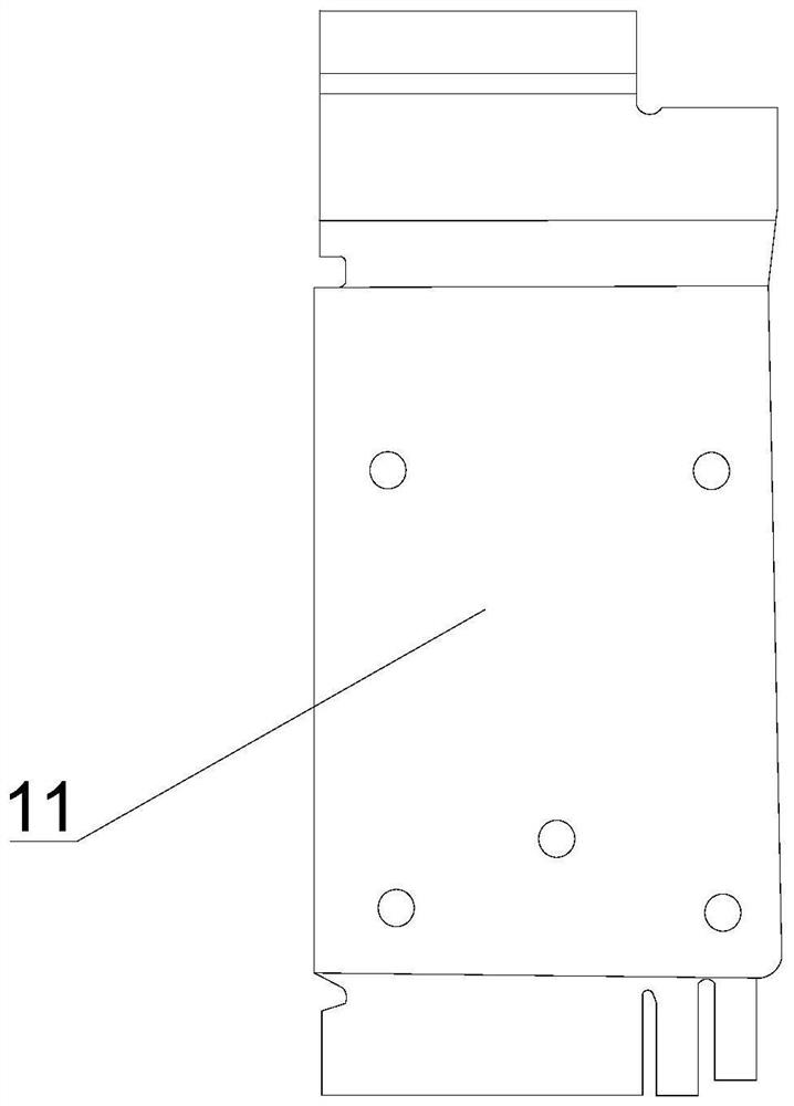
[0067] The removal step includes the mold seal body removal step 1 and the metal layer removal step. In the mold seal body removal step 1, a mixed solution of concentrated nitric acid and concentrated sulfuric acid is used to remove the mold seal body 11 on the surface of the chip body 10. After the mold seal body is removed, the product is as follows: Figure 4 and Figure 5 shown. In the above-mentioned steps, the concentration of concentrated nitric acid is 98%, the concentration of concentrated sulfuric acid is 95%, and the mixing ratio of concentrated nitric acid and concentrated sulfuric acid is 5:1, certainly, the con...

Embodiment 2

[0076] Such as figure 1 , Figure 9 and Figure 10 As shown, in this solution, the side of the chip body 10 facing the lens of the low-light microscope is the back side 102, and the back side 102 of the chip is marked by the imaging marking device, that is, the method for marking the back side 102 of the chip. The specific steps are as follows:

[0077] Removal step: remove the protective layer on the surface of the semiconductor device, such as metal layer, molded body and ceramic layer, etc., the removal method is selected according to the different materials to be removed, such as grinding, chemical corrosion or laser unsealing, etc., which are not included in this application There is no limit, just thin the back of the chip to 150-200um. The processed chip will be transported to the imaging marking device for imaging marking processing, the specific steps are as follows:

[0078] The first positioning step 4: power on the chip body 10 under the low-magnification lens o...


PUM


Abstract

The invention discloses a chip failure positioning method and a clamp. The chip failure positioning method comprises a transfer step, a first positioning step, a first marking step, a second positioning step and a second marking step, and the chip failure positioning method can position failure points of chips with regular surfaces and without characteristic patterns.

Description

technical field [0001] The invention relates to the technical field of deep failure location of semiconductor chips, in particular to a chip failure location method and a fixture. Background technique [0002] For the chip of a failed semiconductor device, it is generally necessary to cut the failure point so as to expose the internal structure of the chip, so as to facilitate observation and analysis of the cause of failure. Before cutting, it is first necessary to determine the location of the failure point. [0003] The failure point location technology provided by the prior art generally includes the following steps: placing the chip on the EMMI (Emission Microscope, low-light microscope) / OBIRCH (Optical Beam Induced Resistance Change, laser beam resistance anomaly detection) device and powering it on, so that it can show The image of the failure point, these are existing mature technologies, and will not be described here. For general chips, due to the complex pattern...

Claims


Application Information

Patent Timeline
IPC IPC(8): G01R31/311G01R31/28G01R1/04
CPCG01R1/0425G01R31/2898G01R31/311
Inventor 龚瑜黄彩清游俊
Owner SHENZHEN STS MICROELECTRONICS
Why Eureka
Try Eureka