
Communication circuit and electronic equipment

A communication circuit and communication channel technology, applied in the field of communication circuits and electronic equipment, can solve the problems of increasing chip area, increasing chip cost, unfavorable size miniaturization, etc., to reduce chip area, improve utilization rate, and facilitate size The effect of miniaturization

Active Publication Date: 2021-01-22
SHANGHAI YAOHUO MICROELECTRONICS CO LTD
View PDF11 Cites 1 Cited by
  • Summary
  • Abstract
  • Description
  • Claims
  • Application Information

AI Technical Summary

Problems solved by technology

At present, in order to add other necessary functions to this type of circuit, the main way is to add extra pins to realize the corresponding functions, which will increase the chip area, increase the cost of the chip, and is not conducive to size miniaturization

Method used


Image

  • Communication circuit and electronic equipment
  • Communication circuit and electronic equipment
  • Communication circuit and electronic equipment

Examples


Embodiment Construction

[0049] The following will clearly and completely describe the technical solutions in the embodiments of the present invention with reference to the accompanying drawings in the embodiments of the present invention. Obviously, the described embodiments are only some, not all, embodiments of the present invention. Based on the embodiments of the present invention, all other embodiments obtained by persons of ordinary skill in the art without making creative efforts belong to the protection scope of the present invention.

[0050] The terms "first", "second", "third", "fourth", etc. (if any) in the description and claims of the present invention and the above drawings are used to distinguish similar objects and not necessarily Describe a specific order or sequence. It is to be understood that the data so used are interchangeable under appropriate circumstances such that the embodiments of the invention described herein can be practiced in sequences other than those illustrated or...


PUM


Abstract

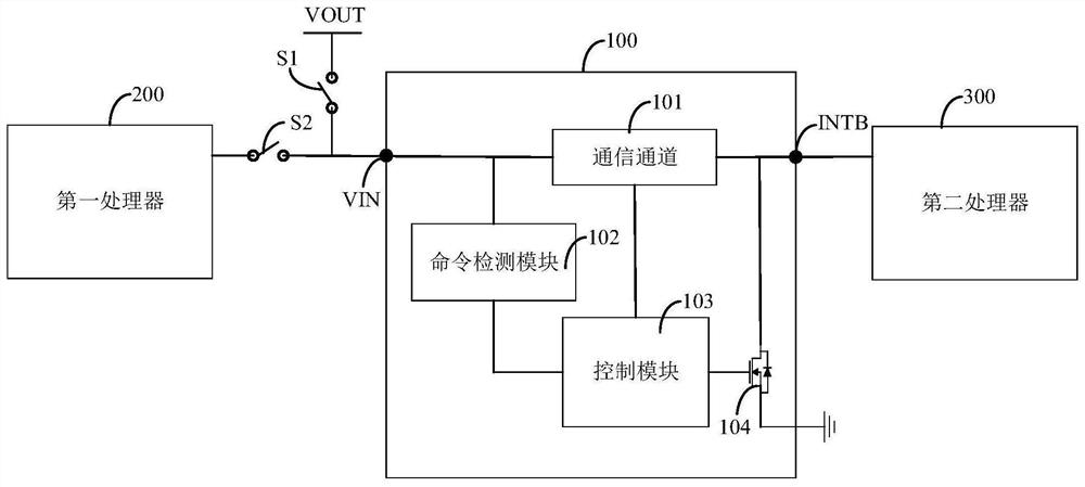
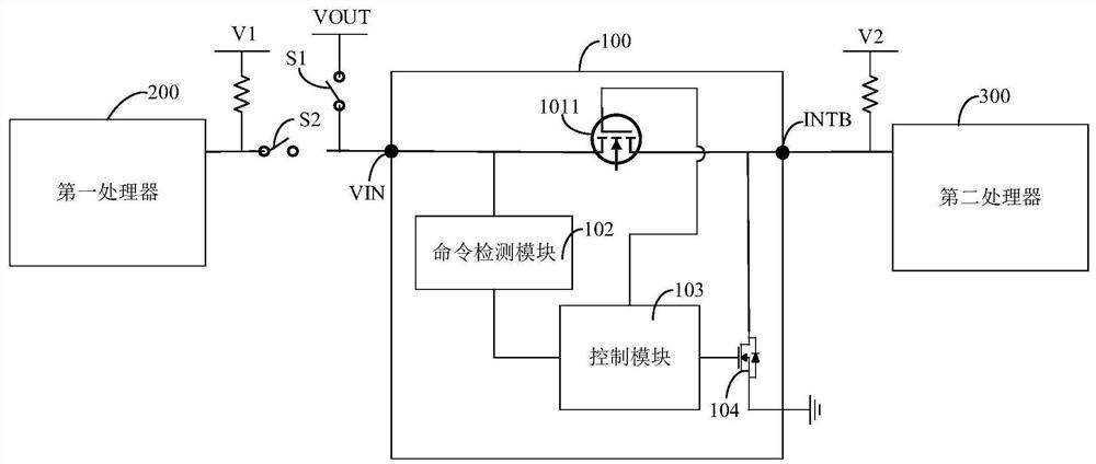
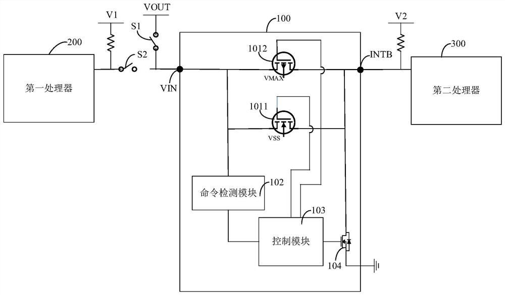
According to the communication circuit and the electronic equipment provided by the invention, the circuit function is newly added by multiplexing the power supply input pin and the interrupt pin, sothat the size miniaturization is facilitated. The communication circuit is provided with a power input pin and an interrupt pin; the power input pin is connected with a first IO port of the first processor through a first switch; the interrupt pin is connected with a second IO port of the second processor; the communication circuit comprises a communication channel, a command detection module anda control module. The communication channel is connected between the power supply input pin and the interrupt pin; the command detection module is used for outputting a first notification signal to the control module when detecting that the power input pin receives a logic control command output from the first IO port; and the output end of the control module is connected with the switching circuit, and the control module is used for controlling the communication channel to be communicable in response to the first notification signal so as to realize communication between the first IO port andthe second IO port through the power input pin, the communication channel and the interrupt pin.

Description

technical field [0001] The invention relates to the technical field of circuits, in particular to a communication circuit and electronic equipment. Background technique [0002] With the rise of true wireless Bluetooth headsets (TWS), wearable watches / bracelets, and small Internet of Things devices, the requirements for such devices are getting higher and higher. In particular, it is increasingly hoped that the size of the internal chips in such devices should be as small as possible small. For small-sized chips, considering that the pin spacing cannot be smaller (for example, the pin spacing of WLP (Wafer Level Package, Wafer Level Package) is usually at least 0.4mm), the number of pins required to realize all functions of the chip often becomes a constraint A key factor in chip area. [0003] With IIC (or called I 2 C (or I2C, that is, the international general integrated circuit communication digital interface) interface circuit, in order to realize the function of the...

Claims


Application Information

Patent Timeline
Patent Type & Authority Applications(China)
IPC IPC(8): H03K19/0175
CPCH03K19/0175
Inventor 黄雷
Owner SHANGHAI YAOHUO MICROELECTRONICS CO LTD
Learn More