Delay line structure and delay jitter correction method thereof

A technology of delay jitter and delay line, which is applied in the direction of automatic power control, logic circuit with logic function, receiver monitoring, etc., to achieve the effect of reducing delay jitter

Active Publication Date: 2021-01-29
SUZHOU MOTORCOMM ELECTRONICS TECH CO LTD
View PDF6 Cites 3 Cited by
  • Summary
  • Abstract
  • Description
  • Claims
  • Application Information

AI Technical Summary

Problems solved by technology

Traditional digital interfaces transmit data only on the rising or falling edge of the clock

Method used


Image

  • Delay line structure and delay jitter correction method thereof
  • Delay line structure and delay jitter correction method thereof
  • Delay line structure and delay jitter correction method thereof

Examples


Embodiment

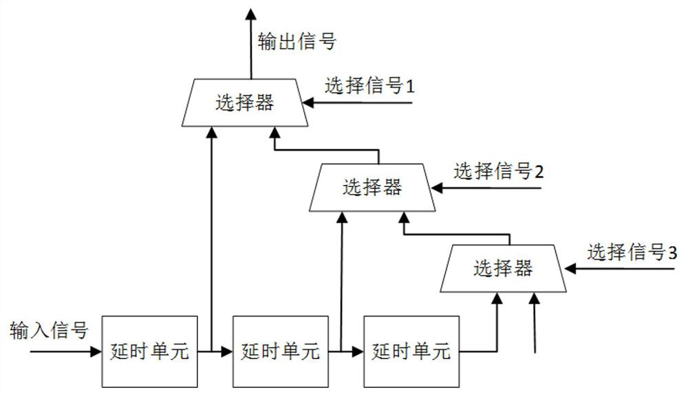
[0029] see figure 2 As shown, the present invention relates to a delay line structure, which is implemented based on a selector, specifically, includes N delay units and N selectors, wherein the output of the N-1th delay unit The terminals are respectively connected to the first input end of the N-1th selector and the input end of the Nth delay unit, the N-1th selector inputs the N-1th selection signal, and the Nth delay unit The output end is connected to the first input end of the Nth selector, the output end of the Nth selector is connected to the second input end of the N-1th selector, and the Nth selector inputs the Nth selection signal, The delay units and the selectors are stacked forward according to the above rules, until the input end of the first delay unit is connected to the input signal and the output end of the first selector is connected to the output signal.

[0030] Assuming that the delay of the combination of a delay unit and the selector in the above del...


PUM


Abstract

The invention discloses a delay line structure and a delay jitter correction method thereof. The delay line structure comprises N delay units and N selectors. The output end of the N-1th delay unit isconnected to the first input end of the N-1th selector and the input end of the Nth delay unit, the N-1th selector inputs the N-1th selection signal, and the N-1th selector outputs the N1th selectionsignal; the output end of the Nth time delay unit is connected to the first input end of the Nth selector, the output end of the Nth selector is connected to the second input end of the N1th selector, and the Nth selector inputs an Nth selection signal. The time delay units and the selectors are stacked forwards according to the rule until the input ends of the first time delay units are connected with input signals and the output ends of the first selectors are connected with output signals. According to the structure, delay control can be carried out on the clock at the sending end or the receiving end to meet the requirement of receiving timing, and the jitter of the delay of the delay line can be reduced.

Description

technical field [0001] The invention relates to the technical field of digital communication, in particular to a delay line structure and a correction method for delay jitter thereof. Background technique [0002] In modern communication networks, due to the increase in data rate, the transmission rate of the chip interface is getting faster and faster. Traditional digital interfaces transmit data only on the rising or falling edge of the clock. In order to increase the transmission rate, on the premise of not changing the clock frequency, data is transmitted on the rising and falling edges of the data at the same time, and the data transmission rate will be doubled. Take the timing sequence of the Ethernet transmission interface RGMII as an example, see figure 1 As shown, RXC is the associated clock, and RXD / RX_CTL is the associated data. It can be seen that the data jumps on the rising and falling edges of RXC. Assuming that the transition edge of the RXC at the sending...

Claims


Application Information

Patent Timeline
Patent Type & Authority Applications(China)
IPC IPC(8): H04L12/26H04B17/21H03K17/28
CPCH04L43/087H04B17/21H03K17/28H03K5/131H03K5/134H03K5/15046H03K5/1252H03K2005/00195H03K19/20H03L7/081
Inventor 刘亚欢
Owner SUZHOU MOTORCOMM ELECTRONICS TECH CO LTD
Why Eureka
Try Eureka