Light-operated semiconductor switch

A semiconductor and switch technology, applied in the field of light-controlled semiconductor switches, can solve the problems of photoconductive switch dependence, inability to adapt to miniaturization requirements, slow turn-on speed, etc., to improve anti-electromagnetic interference ability, increase current conduction uniformity, reduce The effect of small delay jitter

Pending Publication Date: 2020-04-28
INST OF FLUID PHYSICS CHINA ACAD OF ENG PHYSICS
View PDF0 Cites 2 Cited by
  • Summary
  • Abstract
  • Description
  • Claims
  • Application Information

AI Technical Summary

Problems solved by technology

The existing electronically controlled power semiconductor switch cannot be separated from the trigger structure and the main circuit structure, resulting in poor withstand voltage level, reliability, and anti-peak ability, which limits its application in high-power applications; the existing light-controlled thyristor , its turn-on speed is slow and cannot be applied to pulse power applications; the existing photoconductive switch largely relies on the pulse charging auxiliary system or a large-volume laser system, which cannot meet the requirements of miniaturization

Method used


Image

  • Light-operated semiconductor switch
  • Light-operated semiconductor switch
  • Light-operated semiconductor switch

Examples


Embodiment 1

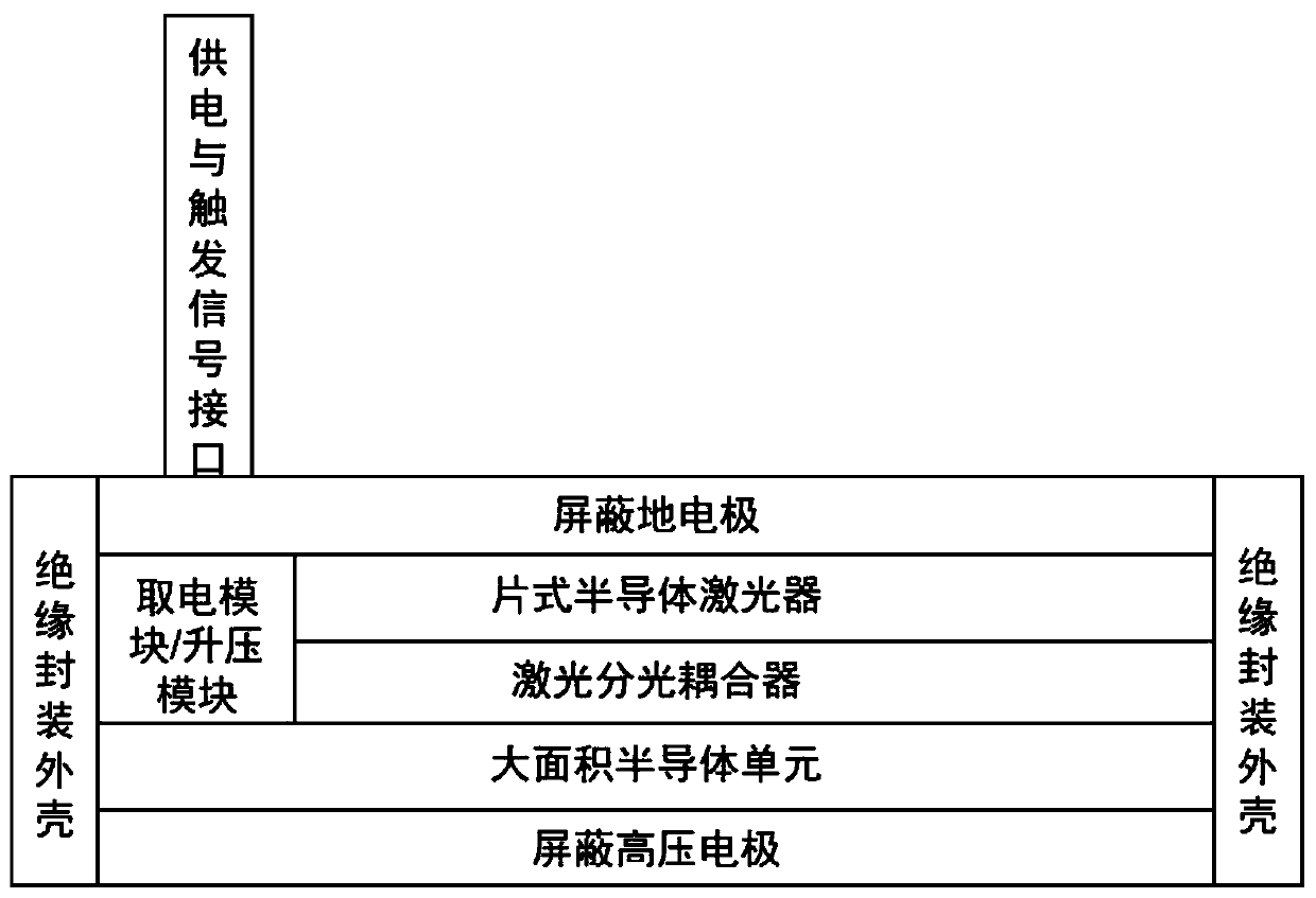
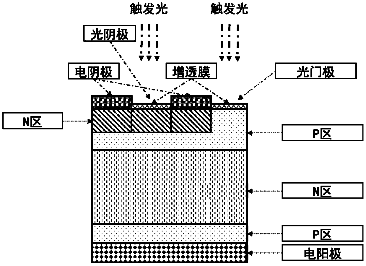
[0055] Apply a high voltage between the shielding ground electrode and the shielding high voltage electrode, the voltage range of the high voltage is 1kV ~ 12kV; the working current range is: 0 ~ 50kA; on this basis, the voltage range can be increased by series connection. Use parallel connection or increase the chip area to increase the working current range.

[0056] In the light-controlled semiconductor switch, the shielding high-voltage electrode is applied to a positive high-voltage point, and the shielding ground electrode is applied to a point or a floating low potential. There is no conduction between them, they can withstand high forward voltage and withstand high reverse voltage.

[0057]When the voltage is applied to the power supply of the optically controlled semiconductor switch and the pulse waveform is given by the trigger signal interface, the chip semiconductor laser will start to work at this time, and the high-current laser drive module in the chip semicond...

Embodiment approach

[0060] After the power supply and trigger signal are introduced into the chip semiconductor laser, a preferred implementation mode: the circuit substrate places most of the components of the high-current laser drive module on the top layer, and places most of the components of the semiconductor laser unit on the bottom layer.

[0061] The high-current laser drive module preferably uses MCT, IGBT or power MOSFET as the discharge switch, and the solid capacitor as the energy storage element. The pulse current is generally between 5A and 500A, and the output is positive pulse or negative pulse. The energy required by the current can be obtained in two ways: high-voltage power extraction and low-voltage boost.

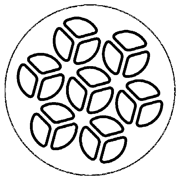
[0062] The laser diode chips are evenly distributed on the circuit substrate according to the requirements, and connected in series, parallel or series-parallel combination, and the positive and negative electrodes are drawn out. The positive and negative electrodes are con...


PUM


Abstract

The invention discloses a light-operated semiconductor switch. A shielding ground electrode, a chip semiconductor laser, a laser beam splitting coupler, a large-area semiconductor unit and a shieldinghigh-voltage electrode are sequentially arranged in the light-operated semiconductor switch from top to bottom. An electricity taking module or a boosting module is connected in a gap between the chip semiconductor laser and the laser beam splitting coupler; the side face of the light-operated semiconductor switch is wrapped with an insulating packaging shell, and the insulating packaging shell and the shielding electrode jointly form a light-operated semiconductor switch packaging shell. A power supply and trigger signal interface of the light-operated semiconductor switch extends out of thelight-operated semiconductor switch packaging shell. According to the invention, the light-operated semiconductor switch can be used for various occasions such as a high-power pulse power supply, a compact high-power pulse assembly, small-size high-energy pulse triggering and the like, and has the advantages of high power capacity, high reliability, long service life, small size and the like.

Description

technical field [0001] The invention belongs to the technical field of pulse power, and in particular relates to a light-controlled semiconductor switch. Background technique [0002] As high-power pulse power supplies and high-power pulse components have put forward requirements for long life, fast frontier, high reliability, and compactness, new solid-state switching technologies with such advantages are very important. The existing electronically controlled power semiconductor switch cannot be separated from the trigger structure and the main circuit structure, resulting in poor withstand voltage level, reliability, and anti-peak ability, which limits its application in high-power applications; the existing light-controlled thyristor , its turn-on speed is slow, and cannot be applied to pulse power applications; the existing photoconductive switch largely depends on the pulse charging auxiliary system or a large-volume laser system, and cannot meet the requirements of min...

Claims


Application Information

Patent Timeline
Patent Type & Authority Applications(China)
IPC IPC(8): H03K17/94H01L31/111
CPCH01L31/1113H03K17/941
Inventor 谢卫平袁建强王凌云刘宏伟
Owner INST OF FLUID PHYSICS CHINA ACAD OF ENG PHYSICS
Why Eureka
Try Eureka