Washing device for optical communication chip production

A cleaning device and chip cleaning technology, which is applied in the direction of using liquid cleaning methods, cleaning methods and utensils, chemical instruments and methods, etc., can solve the problems of low cleaning efficiency and achieve the effect of improving cleaning efficiency and facilitating collection and arrangement

Inactive Publication Date: 2021-02-05
肖国强
View PDF0 Cites 2 Cited by
  • Summary
  • Abstract
  • Description
  • Claims
  • Application Information

AI Technical Summary

Problems solved by technology

[0003] The existing chip cleaning device usually puts all the chips into the cleaning frame for cleaning. If there are many kinds of chips, it needs to be cleaned in batches, and the cleaning efficiency is low. Therefore, a kind of optical communication chip production is proposed. The cleaning device can clean a large number of chips at the same time, and can also clean multiple types of chips at the same time

Method used


Image

  • Washing device for optical communication chip production
  • Washing device for optical communication chip production
  • Washing device for optical communication chip production

Examples


Embodiment 1

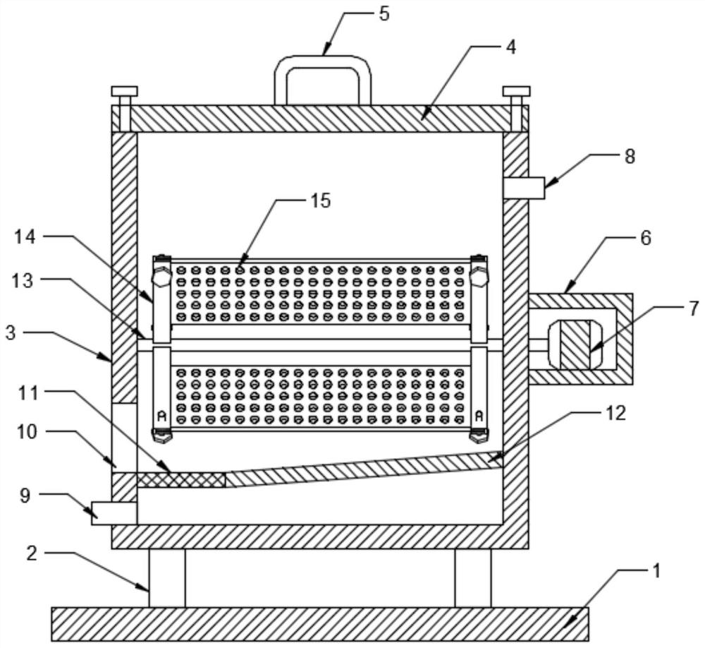
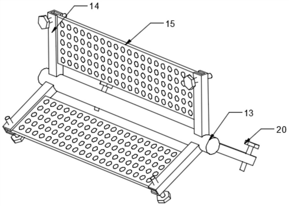
[0025] see Figure 1-5 , a cleaning device for optical communication chip production, comprising a base plate 1, a support column 2 and a cleaning frame 3, a water inlet 8 is provided on one side of the cleaning frame 3, and the cleaning frame 3 is provided with a chip cleaning assembly, and the chip cleaning assembly The specific type is not limited. In this embodiment, preferably, the chip cleaning assembly includes a protective frame 6, a drive motor 7, and a rotating shaft 13. The driving motor 7 is installed in the protective frame 6 and the output end is driven and connected to one end of the rotating shaft 13. The rotating shaft 13 is rotatably installed in the cleaning frame 3 and there are multiple groups of chip placement components arranged on the periphery. The specific type of the chip placement components is not limited. In this embodiment, preferably, the chip placement components include a fixed rod 14 and a placement plate 15 , fastening bolts 20, installation...

Embodiment 2

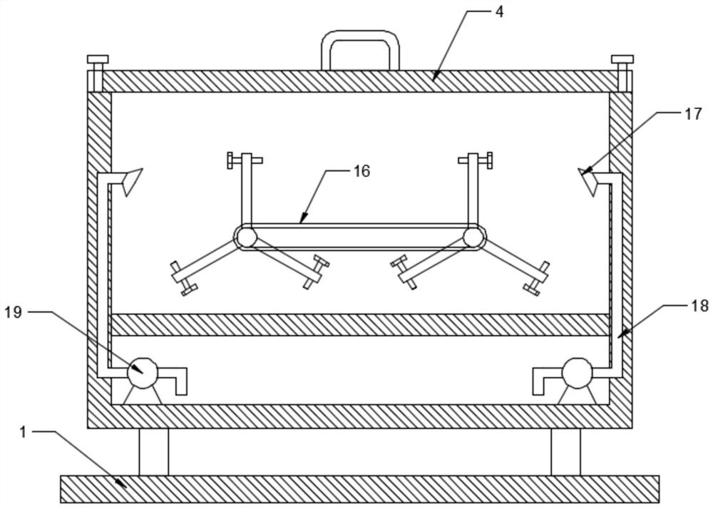
[0034] In order to improve the practicability, this embodiment is further improved on the basis of embodiment 1. The improvement is that: a repeated cleaning component is arranged under the cleaning frame 3, and the specific type of the repeated cleaning component is not limited. In this embodiment , preferably, the repeated cleaning assembly includes a cleaning door 10, a filter screen 11, a deflector 12, a nozzle 17, a water pipe 18 and a water pump 19, and the deflector 12 is installed obliquely in the cleaning frame 13 and between the low end and the cleaning frame 3 A filter screen 11 is arranged between them, a water pump 19 is installed at the bottom of the cleaning frame 3 and is connected with a nozzle 17 through a water pipe 18, the nozzle 17 is located on the side wall of the cleaning frame 3 and facing the placement plate 15, and the cleaning door 10 is opened on the filter On the side of the net 11, during the cleaning process, the cleaning liquid passes through th...


PUM


Abstract

The invention discloses a washing device for optical communication chip production. The washing device comprises a bottom plate, supporting columns and a washing frame, wherein a water adding openingis formed in one side of the washing frame, the washing frame is provided with a chip washing assembly, the chip washing assembly comprises a protection frame, a driving motor and rotating shafts, thedriving motor is installed in the protection frame, the output end of the driving motor is in driving connection with one end of each rotating shaft, each rotating shaft is rotationally installed inthe washing frame, a plurality of groups of chip containing assemblies are arranged on the periphery, and comprise fixing rods, containing plates, fastening bolts, mounting grooves, containing groovesand washing holes, the two fixing rods are symmetrically mounted at two ends of the corresponding rotating shaft and provided with mounting grooves, two ends of the containing plates are movably mounted in the mounting grooves, the tops are fixed in the mounting grooves through the fastening bolts, the plurality of containing grooves are horizontally formed in one sides of the containing plates,and washing holes are formed in two side walls of the containing grooves. By arranging the chip washing assembly and the chip containing assemblies, the washing efficiency, washing quality and practicability are greatly improved.

Description

technical field [0001] The invention relates to the field of preparation of optical communication devices, in particular to a cleaning device for the production of optical communication chips. Background technique [0002] Optical communication is a communication method in which light waves are used as carriers. There are two ways to increase the bandwidth of the optical path: one is to increase the single-channel transmission rate of an optical fiber; the other is to increase the number of wavelengths transmitted in a single optical fiber, that is, wavelength division multiplexing technology; in the field of optical communication, devices need to be produced, and chips are An essential one that requires cleaning after chip production. [0003] The existing chip cleaning device usually puts all the chips into the cleaning frame for cleaning. If there are many kinds of chips, it needs to be cleaned in batches, and the cleaning efficiency is low. Therefore, a kind of optical ...

Claims


Application Information

Patent Timeline
Patent Type & Authority Applications(China)
IPC IPC(8): B08B3/10B08B3/02B08B13/00
CPCB08B3/022B08B3/041B08B3/10B08B13/00
Inventor 肖国强
Owner 肖国强
Why Eureka
Try Eureka