
Method for assisting waveform debug in chip verification and application

An auxiliary waveform and chip technology, applied in the field of chip development, can solve problems such as difficult verification personnel, time consumption of verification personnel, and reduced debugging efficiency, so as to achieve the effect of improving efficiency

Pending Publication Date: 2021-02-09
MOLCHIP TECH (SHANGHAI) CO LTD
View PDF0 Cites 0 Cited by
  • Summary
  • Abstract
  • Description
  • Claims
  • Application Information

AI Technical Summary

Problems solved by technology

Considering that under normal circumstances, a test case may include a large number of test configuration files. If the verifier visually checks the waveform file and manually converts the configuration information, it will consume a lot of time for the verifier, making it difficult for the verifier to quickly and accurately determine the target that needs to be debugged. , reducing the debugging efficiency

Method used


Image

  • Method for assisting waveform debug in chip verification and application
  • Method for assisting waveform debug in chip verification and application
  • Method for assisting waveform debug in chip verification and application

Examples


Embodiment

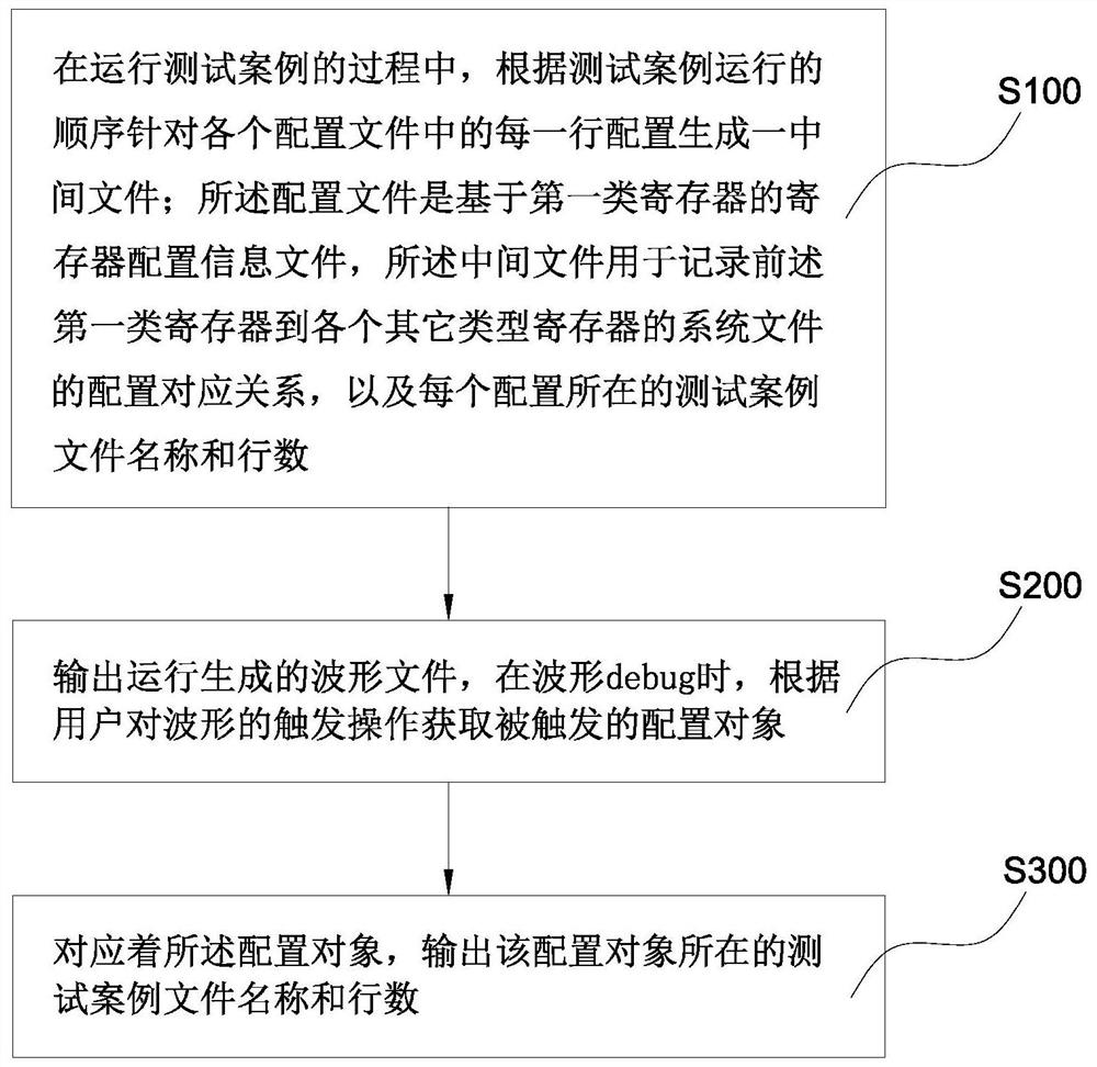
[0038] see figure 1 and figure 2 As shown, a method for auxiliary waveform debugging (error detection, or error debugging) in a chip verification provided by the present invention, the method includes the following steps:

[0039]S100, in the process of running the test case, generate an intermediate file for each line configuration in each configuration file according to the order of test case (case test) operation; the configuration file is a register configuration information file based on the first type of register, The intermediate file is used to record the configuration correspondence between the aforementioned first-type registers and system files of other types of registers, as well as the test case file name and line number where each configuration is located.

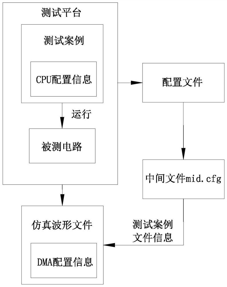
[0040] see figure 2 As shown, in the test platform, a test case (case test) is run through the circuit under test for simulation, and a simulation waveform file is generated. During the running of the te...


PUM


Abstract

The invention discloses a method for assisting waveform debug in chip verification and application, and relates to the technical field of chip development. The method comprises the following steps: inthe process of running a test case, generating an intermediate file for each row of configuration in each configuration file according to the running sequence of the test case, wherein the configuration file is a register configuration information file based on a first type register, and the intermediate file is used for recording a configuration corresponding relationship from the first type register to system files of other types of registers, and a name and a row number of a test case file where each configuration is located; and outputting a waveform file generated by operation, obtaininga triggered configuration object according to a triggering operation of a user on the waveform when the waveform is debug, and outputting the name and the line number of the test case file where theconfiguration object is located. According to the invention, a user can clearly and visually obtain the target object information needing debug, and the user does not need to perform manual conversionand query.

Description

technical field [0001] The invention relates to the technical field of chip development, in particular to a method and application of auxiliary waveform debugging in chip verification. Background technique [0002] In the field of chip design, verification (Verification) runs through the entire design process. From behavioral HDL design to chip tape-out (TAPE-OUT), a large number of EDA (Eletronic Design Automation, electronic design automation) verifications are required. Currently, verification Work has accounted for about 70% of the entire design work. When the result of EDA verification does not match the target performance of the chip design, it is necessary to find out the defect in the chip design and repair it. Among them, the test case (case test) is simulated and the FSDB (Fast Signal Data Base) file is generated, and the bug (defect) is located and corrected through the waveform debug (debug, or debug) tool such as Verdi (after correction, Simulation again) is a...

Claims


Application Information

Patent Timeline
Patent Type & Authority Applications(China)
IPC IPC(8): G06F11/22
CPCG06F11/2273G06F11/2289
Inventor 袁力胡扬央
Owner MOLCHIP TECH (SHANGHAI) CO LTD
Learn More