Conductive substrate and electrochromic device

A technology of electrochromic devices and conductive substrates, applied in instruments, nonlinear optics, optics, etc., can solve problems such as uneven discoloration of electrochromic devices

Active Publication Date: 2021-02-12
SHENZHEN GUANGYI TECH CO LTD
View PDF3 Cites 1 Cited by
  • Summary
  • Abstract
  • Description
  • Claims
  • Application Information

AI Technical Summary

Problems solved by technology

[0005] An embodiment of the present invention provides a conductive substrate and an electrochromic device, so as to solv

Method used


Image

  • Conductive substrate and electrochromic device
  • Conductive substrate and electrochromic device
  • Conductive substrate and electrochromic device

Examples


Embodiment 1

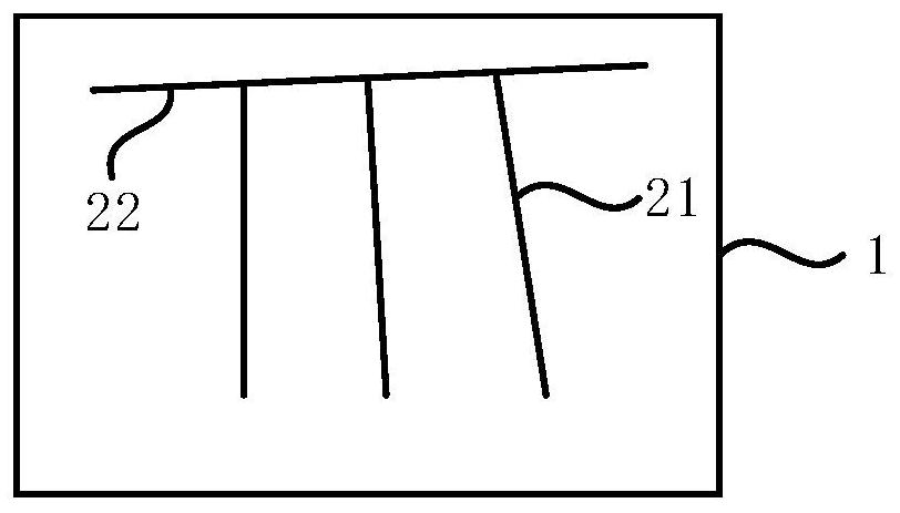
[0051] Embodiment 1 of the present invention provides a conductive substrate, the conductive substrate includes: a base layer, a conductive layer, and a wiring layer; wherein, the conductive layer is disposed on the base layer; the wiring layer is disposed on the conductive layer, and the wiring layer includes The first conductive circuit arranged in the first direction and the second conductive circuit arranged in the second direction, such as figure 1 As shown, the first conductive circuit 21 extends inward from the edge of the conductive layer 1 , the second conductive circuit 22 is disposed on the edge of the conductive layer 1 , and the first conductive circuit 21 and the second conductive circuit 22 are electrically connected.

[0052] Wherein, the base layer may be a transparent base, and is an optical grade transparent material, specifically, a flexible base material, including polyester film (Polyester Film, PET), cycloolefin copolymer, or cellulose triacetate. The cond...

Embodiment 2

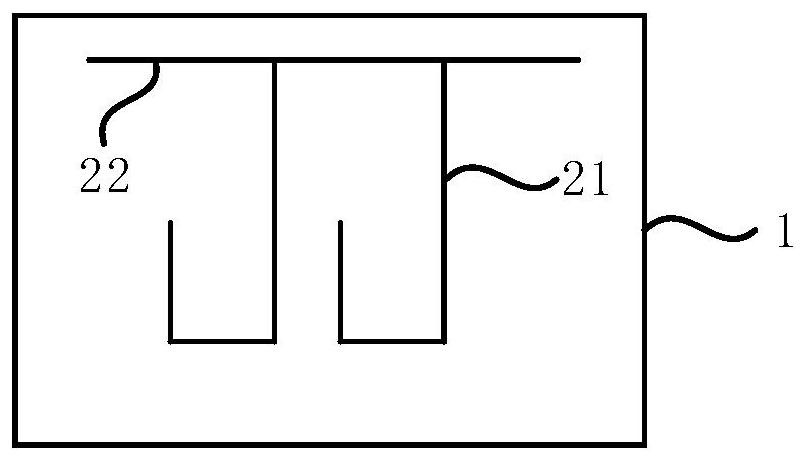
[0062] Embodiment 2 of the present invention provides a conductive substrate. The technical solution of this embodiment is further refined on the basis of the technical solution of the above embodiment, optionally, such as Image 6 As shown, the wiring layer further includes: an extraction structure 23 electrically connected to the second conductive circuit 22 . Specifically, the material of the lead-out structure 23 can be the same as that of the second conductive circuit 22, and the shape can be L-shaped, I-shaped, T-shaped, etc., connected to the second conductive circuit 22, or a structural extension of the second conductive circuit 22, When applied to an electrochromic device, it can be used to replace the second conductive line 22 to connect with the lead-out electrode, thereby avoiding damage to the second conductive line 22 and reducing the difficulty of welding. Optionally, there is only one lead-out structure 23 , which can be connected to one end or the center of t...

Embodiment 3

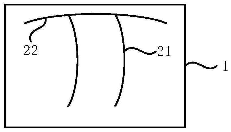
[0066] Embodiment 3 of the present invention provides a conductive substrate. The technical solution of this embodiment is further refined on the basis of the technical solution of the above embodiment, optionally, such as Figure 9 As shown, the end of the first conductive circuit 21 includes bifurcated structures 211 arranged symmetrically. Specifically, since when applied to an electrochromic device, the end of the first conductive line 21 usually does not diffuse the discolored area outwards in a rectangle, but diffuses in a circular arc shape, even if it has been completed in other aspects Optimizing, there will always be a region where the discoloration is always slow in the non-overlapping part of the rectangle and the arc shape. Therefore, by setting the end of the first conductive line 21 as a symmetrical bifurcated structure 211, the slow discoloration can be effectively reduced. area, thereby further improving the uniformity of the overall discoloration. preferred...


PUM


Abstract

The embodiment of the invention discloses a conductive substrate and an electrochromic device. The conductive substrate comprises a substrate layer, a conductive layer and a wiring layer; the conductive layer is arranged on the substrate layer; the wiring layer is arranged on the conductive layer and comprises a first conductive circuit arranged in a first direction and a second conductive circuitarranged in a second direction, the first conductive circuit extends inwards from the edge of the conductive layer, the second conductive circuit is arranged on the edge of the conductive layer, andthe first conductive circuit is electrically connected with the second conductive circuit. According to the technical scheme provided by the embodiment of the invention, the potential difference between the edge and the center of the conductive substrate is reduced when the conductive substrate is electrified, so that when the conductive substrate is applied to the electrochromic device, the halophenomenon is weakened, a more uniform color changing process is realized, and meanwhile, especially for the electrochromic device with a relatively large area, a relatively high color changing speedis ensured.

Description

technical field [0001] The embodiments of the present invention relate to the field of electrochromic technology, in particular to a conductive substrate and an electrochromic device. Background technique [0002] Electrochromism is a phenomenon in which the optical properties of materials undergo a stable and reversible color change under the action of an applied electric field. It is manifested as a reversible change in color and transparency in appearance. It is widely used in optical devices, lamps, glass products and decorations. Has a very wide range of applications. [0003] In the prior art, the wiring of the electrochromic device is arranged on the edge of the device. Therefore, especially for a large-area electrochromic device, since the transparent conductive layer of the electrochromic device has a certain square resistance, the wiring applied on the edge When the voltage is transmitted to the center of the device, it will be less than the applied voltage value,...

Claims


Application Information

Patent Timeline
IPC IPC(8): G02F1/153
CPCG02F1/1533
Inventor 王巍舒
Owner SHENZHEN GUANGYI TECH CO LTD
Why Eureka
Try Eureka