Supercharge Your Innovation With Domain-Expert AI Agents!

Chip, programming debugger, system and method for locking programming debugging entry

A debugger and chip technology, applied in software testing/debugging, instrumentation, electrical digital data processing, etc., can solve problems such as conflicts, achieve the effects of reducing costs, saving resources, and enhancing flexibility

Pending Publication Date: 2021-02-19
SHANGHAI EASTSOFT MICROELECTRONICS
View PDF0 Cites 0 Cited by
  • Summary
  • Abstract
  • Description
  • Claims
  • Application Information

AI Technical Summary

Problems solved by technology

However, during the first or secondary development, programming and debugging of the chip, the programming and debugging port often conflicts with the general-purpose port used by the program to run normally.

Method used


Image

  • Chip, programming debugger, system and method for locking programming debugging entry
  • Chip, programming debugger, system and method for locking programming debugging entry
  • Chip, programming debugger, system and method for locking programming debugging entry

Examples


Embodiment Construction

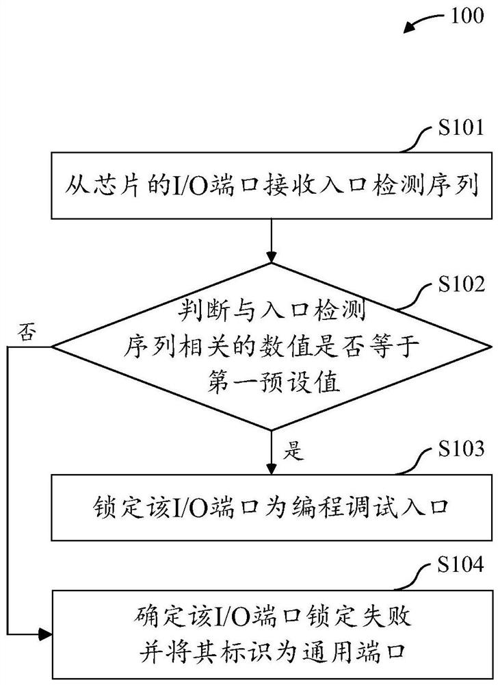
[0051] In the embodiment of the present invention, the chip is a programmable device, for example, it can be a Field-Programmable Gate Array (Field-Programmable Gate Array, FPGA), or a complex programmable logic device (Complex Programmable Logic Device, CPLD), or a microcontroller Controller (Micro-Controller Unit, MCU).

[0052] The I / O port is a pin of the chip, which can be in an input state to receive information sent by an external device or can be in an output state to send information to an external device during normal communication.

[0053] The chip is connected with external devices such as programming debugger through its I / O port.

[0054] First, it is necessary to determine which I / O ports can be used as candidate ports for subsequent port locking operations.

[0055] Specifically, the programming debugger can determine which groups or which I / O ports the chip supports according to the chip specification, and can display these I / O ports as alternative ports on ...


PUM


Abstract

The embodiment of the invention provides a chip, a programming debugger, a system and a method for locking a programming debugging entrance. The method comprises the following steps: S101, receiving an entrance detection sequence from an I / O port of a chip; S102, judging whether the numerical value related to the entrance detection sequence is equal to a first preset value or not: if so, locking the I / O port as a programming debugging entrance, and if not, determining that the I / O port fails to be locked. Compared with the prior art, the embodiment of the invention can provide a plurality of groups or a plurality of I / O ports as alternative ports of the programming debugging entry, so that the flexibility of selection of the programming debugging entry is enhanced; moreover, one group of I / O ports can be locked from a plurality of groups of I / O ports, or one I / O port can be locked from a plurality of I / O ports, so that the port conflict problem in the programming debugging process is avoided.

Description

technical field [0001] The invention relates to the technical field of chip design, in particular to a method for locking a programming and debugging entry, a chip, a programming debugger and a system. Background technique [0002] At present, embedded systems are getting smaller and smaller, and the requirements for the number of chip ports are getting higher and higher, that is, under the same conditions, it is necessary to use the minimum number of input / output (IN / OUT, I / O) ports to meet the maximum application requirements. [0003] In some application scenarios, programmable logic devices and embedded memory chips need to be programmed and debugged. However, during the first or secondary development, programming and debugging of the chip, the programming and debugging port often conflicts with the general-purpose port used by the program to run normally. In order to solve such problems, the present invention proposes a method for multiplexing multiple groups or multi...

Claims


Application Information

Patent Timeline
IPC IPC(8): G06F11/36
CPCG06F11/3656G06F11/362
Inventor 刘桂蓉陈光胜罗文怡赵启山
Owner SHANGHAI EASTSOFT MICROELECTRONICS
Features
  • R&D
  • Intellectual Property
  • Life Sciences
  • Materials
  • Tech Scout
  • Unparalleled Data Quality
  • Higher Quality Content
  • 60% Fewer Hallucinations
Learn More