Check patentability & draft patents in minutes with Patsnap Eureka AI!

Ultrasonic cleaning device, semiconductor equipment and control method of semiconductor equipment

A technology of cleaning device and control method, which is applied in semiconductor/solid-state device manufacturing, cleaning methods and utensils, cleaning methods using liquids, etc. problem, to avoid the effect of uneven cleaning

Inactive Publication Date: 2021-02-23
BEIJING NAURA MICROELECTRONICS EQUIP CO LTD
View PDF6 Cites 0 Cited by
  • Summary
  • Abstract
  • Description
  • Claims
  • Application Information

AI Technical Summary

Problems solved by technology

Multiple ultrasonic transducers are wired in parallel. When one of the ultrasonic transducers is damaged, the other ultrasonic transducers can continue to work normally. However, the ultrasonic output of the damaged ultrasonic transducer is weakened or even stopped, resulting in multiple The ultrasonic waves output by each ultrasonic transducer are no longer consistent, so that when the cleaning step continues, it will cause uneven cleaning on the surface of the workpiece to be cleaned, affecting the cleaning effect

Method used


Image

  • Ultrasonic cleaning device, semiconductor equipment and control method of semiconductor equipment
  • Ultrasonic cleaning device, semiconductor equipment and control method of semiconductor equipment
  • Ultrasonic cleaning device, semiconductor equipment and control method of semiconductor equipment

Examples


Embodiment Construction

[0034]DETAILED DESCRIPTION OF THE PREFERRED EMBODIMENTS It should be understood that the specific embodiments described herein are intended to illustrate and explain the present invention and is not intended to limit the invention.

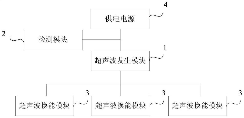
[0035]The embodiment of the present invention provides an ultrasonic cleaning device, which is applied to a semiconductor device.figure 1 A module schematic diagram of an ultrasonic cleaning device provided by an embodiment of the present invention, such asfigure 1 As shown, the ultrasonic cleaning device includes: an ultrasonic wave generating module 1, a detection module 2, and a plurality of parallel ultrasonic transduction modules 3. The ultrasonic occurrence module 1 is connected to the power supply 4 and the plurality of ultrasonic transduction modules 3, and the ultrasonic occurrence module 1 is used to provide a drive signal to each of the ultrasonic transduction modules 3. The ultrasonic transduction module 3 is used to emit ultrasonic waves under...


PUM


Abstract

The invention provides an ultrasonic cleaning device, semiconductor equipment and a control method of the semiconductor equipment, and relates to the technical field of semiconductor processing. The ultrasonic cleaning device comprises an ultrasonic generation module, a detection module and a plurality of ultrasonic transduction modules connected in parallel; the ultrasonic generation module is connected with a power supply and the plurality of ultrasonic transduction modules correspondingly and is used for providing driving signals for the ultrasonic transduction modules, and the ultrasonic transduction modules are used for emitting ultrasonic waves under the driving of the driving signals; and the detection module is connected with the ultrasonic generation module and is used for detecting the working current flowing through the ultrasonic generation module and judging whether an abnormal ultrasonic transduction module exists or not according to the working current, and if yes, an alarm signal is sent out, and the alarm signal is used for prompting that the abnormal ultrasonic transduction module exists. According to the ultrasonic cleaning device, the problem that a to-be-cleaned piece is not cleaned uniformly due to the fact that the ultrasonic transduction modules are abnormal can be solved.

Description

Technical field [0001] The invention relates to the field of semiconductor processing technology, and in particular to an ultrasonic cleaning device, semiconductor equipment and a control method thereof. Background technique [0002] At present, ultrasonic cleaning mainly uses ultrasonic transducers to convert electrical energy into mechanical vibration, so that the liquid in the cleaning tank generates bubbles under the action of ultrasonic waves. When ultrasonic waves propagate in the liquid, the bubbles increase rapidly and then suddenly close. And when the bubbles close, a shock wave is generated, and the impact force can scrub the solid surface. [0003] The ultrasonic cleaning device includes an ultrasonic generator and a plurality of ultrasonic transducers. The ultrasonic generator is used to drive the plurality of ultrasonic transducers to vibrate to emit ultrasonic waves. Multiple ultrasonic transducers are wired in parallel. When one of the ultrasonic transducers ...

Claims


Application Information

Patent Timeline
Patent Type & Authority Applications(China)
IPC IPC(8): B08B3/12B08B13/00H01L21/67
CPCB08B3/12B08B13/00H01L21/67023
Inventor 杨树国张虎张明林立
Owner BEIJING NAURA MICROELECTRONICS EQUIP CO LTD
Features
  • R&D
  • Intellectual Property
  • Life Sciences
  • Materials
  • Tech Scout
  • Unparalleled Data Quality
  • Higher Quality Content
  • 60% Fewer Hallucinations
Learn More