Semiconductor material cleaning device

A cleaning device and a technology for semiconductors, which can be applied to cleaning methods using liquids, manufacturing of semiconductor/solid-state devices, cleaning methods using tools, etc., can solve the problems of low cleaning efficiency, poor cleaning effect, and inability to rinse semiconductor materials, etc. To achieve the effect of improving stability and security

Inactive Publication Date: 2021-03-02
江西舜源电子科技有限公司
View PDF9 Cites 4 Cited by
  • Summary
  • Abstract
  • Description
  • Claims
  • Application Information

AI Technical Summary

Problems solved by technology

The method of simply relying on circulating water for rinsing is relatively simple, and the semiconductor materials located inside cannot be washed well after being stacked, resulting in low cleaning efficiency and poor cleaning effects.

Method used


Image

  • Semiconductor material cleaning device
  • Semiconductor material cleaning device
  • Semiconductor material cleaning device

Examples


Embodiment Construction

[0040] The technical solutions of the present invention will be further described below in conjunction with the accompanying drawings and through specific implementation methods.

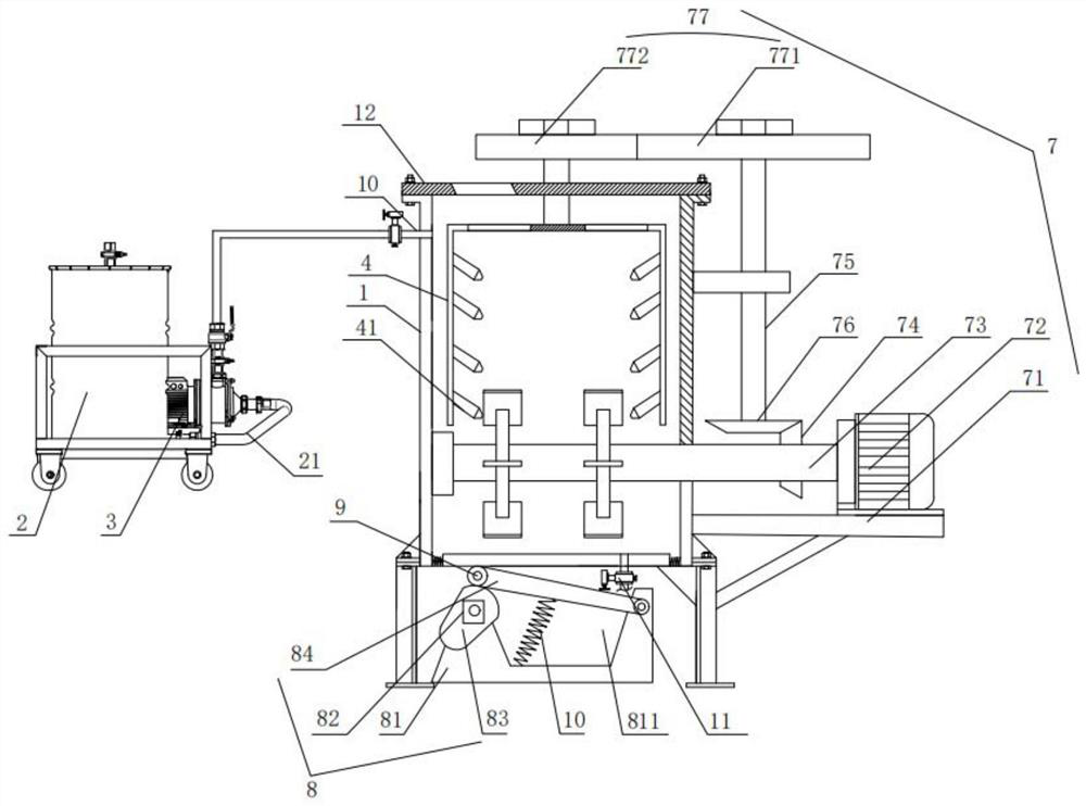
[0041] Figure 1-2 Shown, a cleaning device for semiconductor materials, comprising:

[0042] Cleaning box 1, the cleaning box 1 can clean the semiconductor material layer by layer in the height direction; the bottom of the cleaning box 1 is provided with a vibration plate 11; the vibration plate 11 is elastically arranged at the bottom of the cleaning box 1;

[0043] The liquid storage tank 2 is used to store the cleaning liquid, and pump the cleaning liquid into the cleaning tank 1 through the pump body 3, so as to realize the circular array to wash the semiconductor material layer by layer;

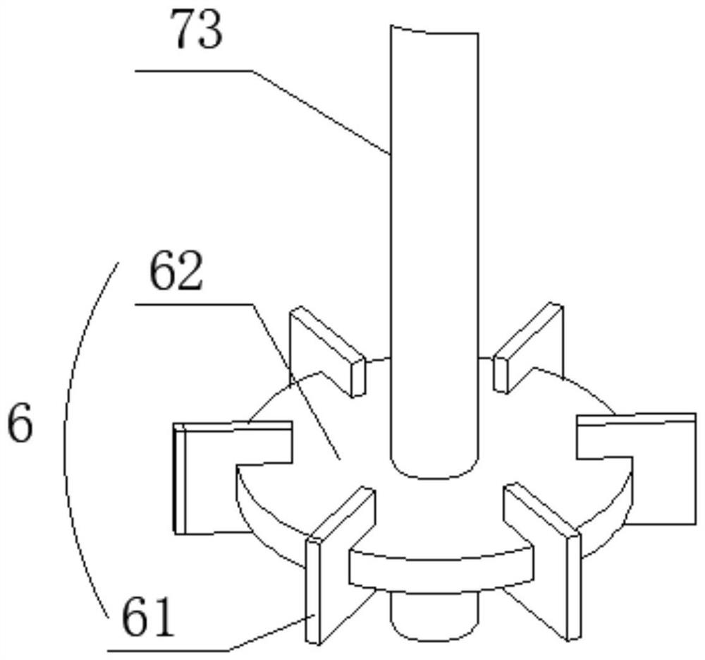
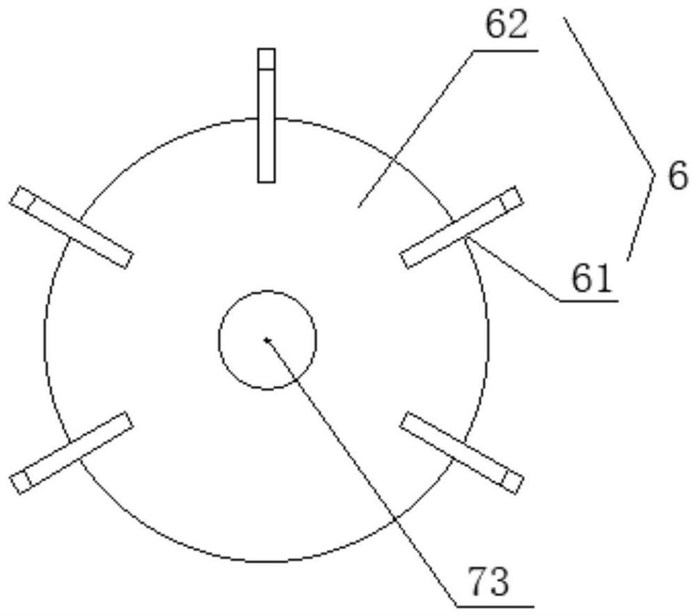
[0044] Circulation dial cylinder body 4 is in the shape of a thin plate cylinder, its top and bottom are open, and a plurality of feed rods 41 are provided on its circumferential inner wall;

[0045] The c...


PUM


Abstract

The invention discloses a semiconductor material cleaning device, which comprises: a cleaning box capable of hierarchically cleaning a semiconductor material in the height direction, a vibrating plateis arranged at the bottom of the cleaning box, and the vibrating plate is elastically arranged at the bottom of the cleaning box; a liquid storage tank which is used for storing cleaning liquid, wherein the cleaning liquid is pumped into the cleaning tank through a pump body, so that the semiconductor material is flushed by layers in a circumferential array manner; a circulating material stirringbarrel which is in a thin-plate cylindrical shape, the top and the bottom of the circulating material stirring barrel are open, wherein a plurality of material stirring rods are arranged on the circumferential inner side wall of the circulating material stirring barrel; cleaning pipeline assemblies which are distributed on the inner side wall of the cleaning box in an annular array mode; a cleaning roller assembly which is located at the bottom of the cleaning box and conducts rolling cleaning on the semiconductor material; a driving part which can simultaneously control the circulating material stirring barrel body and the cleaning roller assembly to synchronously rotate; and a vibration assembly which generates periodic vibration on the vibration plate, wherein overturning and positionreplacement of the semiconductor material are realized by matching with a material stirring rod, and therefore, the semiconductor material can be flushed more cleanly and cleaned more thoroughly, andthe cleaning efficiency and effect are improved.

Description

technical field [0001] The invention relates to the field of cleaning devices, in particular to a cleaning device for semiconductor materials. Background technique [0002] In the current manufacturing process of semiconductor materials, various organic compounds, metal impurities and particles will adhere to the surface of semiconductor materials, and the cleanliness of the surface of semiconductor materials is one of the important factors affecting the reliability of semiconductor devices. If it is not cleaned, it will be greatly reduced. The performance and pass rate of semiconductor devices, so in the manufacturing process of semiconductor devices, 20% of the steps are cleaning of semiconductor materials, removing organic compounds, metal impurities and particles attached to the surface of semiconductor materials, and improving the quality of semiconductor devices. performance and pass rate. [0003] However, in the process of realizing the technical solution of the inv...

Claims


Application Information

Patent Timeline
Patent Type & Authority Applications(China)
IPC IPC(8): H01L21/02H01L21/67B08B3/02B08B3/10B08B1/04B08B1/02
CPCH01L21/67051H01L21/67046H01L21/02052B08B3/02B08B3/022B08B3/10B08B1/002B08B1/04B08B1/02
Inventor 李超
Owner 江西舜源电子科技有限公司
Why Eureka
Try Eureka