
Printed circuit board and electronic equipment

A technology for printed circuit boards and electronic equipment, applied in printed circuits, printed circuit components, electrical components, etc., can solve problems such as reducing the performance of printed circuit boards, simplify circuit design, reduce occupied area, and reduce circuit loss Effect

Pending Publication Date: 2021-04-02
SHENZHEN K FREE WIRELESS INFORMATION TECH
View PDF10 Cites 0 Cited by
  • Summary
  • Abstract
  • Description
  • Claims
  • Application Information

AI Technical Summary

Problems solved by technology

[0004] In view of this, the purpose of the embodiments of the present application is to provide a printed circuit board and electronic equipment to improve the performance of the printed circuit board caused by the same-layer design of the differential pair signal lines in the prior art.

Method used


Image

  • Printed circuit board and electronic equipment
  • Printed circuit board and electronic equipment
  • Printed circuit board and electronic equipment

Examples


Embodiment Construction

[0045] The following will clearly and completely describe the technical solutions in the embodiments of the present application with reference to the drawings in the embodiments of the present application. Apparently, the described embodiments are only some of the embodiments of the present application, but not all of them. Based on the embodiments of the embodiments of the present application, all other embodiments obtained by persons of ordinary skill in the art without making creative efforts belong to the scope of protection of the embodiments of the present application.

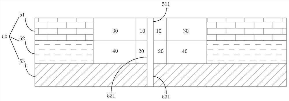
[0046] The embodiment of the present application provides a printed circuit board and electronic equipment. A layered design wiring method is designed on the printed circuit board. Because the differential pair signal line has excellent anti-interference ability, signal integrity and low loss, etc., The V+ and V- signal lines of the differential pair signal lines are respectively arranged on different la...


PUM


Abstract

The invention provides a printed circuit board and electronic equipment, and relates to the technical field of printed circuit boards. The circuit board comprises a first differential pair signal line, a second differential pair signal line, first grounding networks, a second grounding network and a multilayer structure, The multi-layer structure comprises a first-layer structure, a second-layer structure and a main ground layer, the first differential pair signal line is arranged on the first-layer structure, the second differential pair signal line is arranged on the second-layer structure,and the first grounding networks are arranged on the first side and the second side of the first differential pair signal line in the wiring direction. The second grounding network is arranged on thefirst side and the second side of the second differential pair signal line along the wiring direction, and the first differential pair signal line and the second differential pair signal line are respectively connected with the main ground layer. The differential pair signal lines are arranged on the adjacent layer structures of the printed circuit board through layered design, so that the performance of the printed circuit board is optimized.

Description

technical field [0001] The present application relates to the technical field of circuit boards, in particular, to a printed circuit board and electronic equipment. Background technique [0002] With the rapid development of science and technology, various electronic products have begun to develop and upgrade rapidly, and printed circuit boards (Printed Circuit Board, PCB board) are playing an increasingly important role in the electronics industry, occupying an absolute control position. As the physical support of electronic products and an important part of signal transmission, printed circuit boards determine the performance, life cycle and market competitiveness of electronic products. [0003] Among them, the design of differential pair signal lines in printed circuit boards is widely used in the industry for its superior anti-interference ability, signal integrity and low loss. However, in the traditional PCB design of differential pair signal lines, the V+ and V- sig...

Claims


Application Information

Patent Timeline
IPC IPC(8): H05K1/02
CPCH05K1/0245
Inventor 章华王志勇卢余刘富杰冯美银李远高
Owner SHENZHEN K FREE WIRELESS INFORMATION TECH
Features
  • Generate Ideas
  • Intellectual Property
  • Life Sciences
  • Materials
  • Tech Scout
  • Unparalleled Data Quality
  • Higher Quality Content
  • 60% Fewer Hallucinations
Learn More