Supercharge Your Innovation With Domain-Expert AI Agents!

Chip inspection tracking method and device

A chip inspection and tracking device technology, applied in the field of integrated circuits, can solve the problem of inability to track chip model information in different test stages

Active Publication Date: 2021-04-20
HYGON INFORMATION TECH CO LTD
View PDF15 Cites 2 Cited by
  • Summary
  • Abstract
  • Description
  • Claims
  • Application Information

AI Technical Summary

Problems solved by technology

[0004] In view of this, the embodiment of the present invention provides a method and device for chip inspection and tracking, which are used to solve the problem that the chip model information in different test stages cannot be tracked in the existing chip test process. Effective tracking of chip information to ensure the accuracy and consistency of chip models

Method used


Image

  • Chip inspection tracking method and device
  • Chip inspection tracking method and device
  • Chip inspection tracking method and device

Examples


Embodiment Construction

[0079] Embodiments of the present invention will be described in detail below in conjunction with the accompanying drawings.

[0080] It should be clear that the described embodiments are only some of the embodiments of the present invention, not all of them. Based on the embodiments of the present invention, all other embodiments obtained by persons of ordinary skill in the art without creative efforts fall within the protection scope of the present invention.

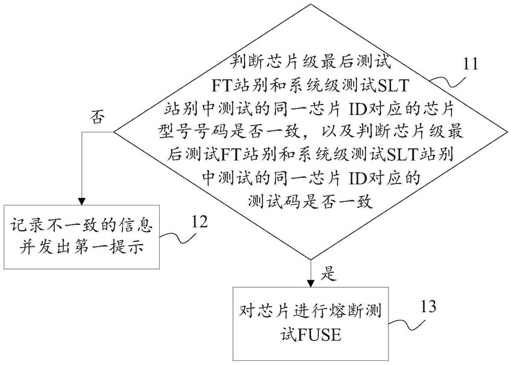
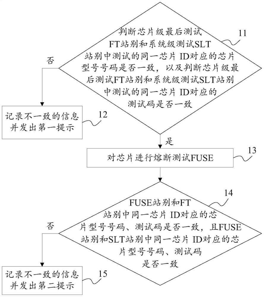
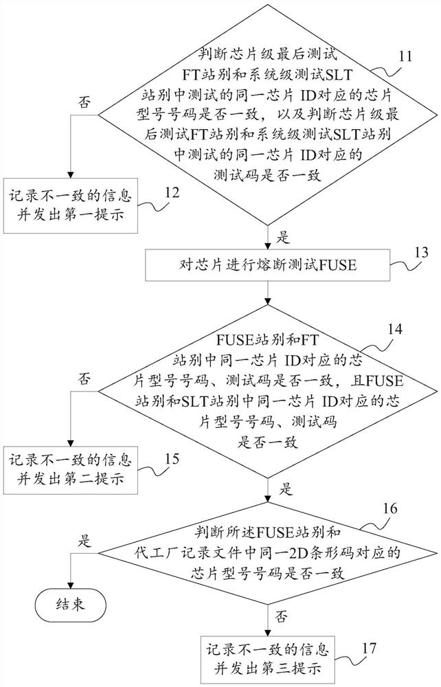
[0081] figure 1 It is a schematic flowchart of Embodiment 1 of a chip inspection and tracking method provided by the present invention. see figure 1 , the method includes the following steps before performing a fuse test on the chip:

[0082] Step 11: Compare and judge whether the chip model number corresponding to the same chip ID tested in the chip-level final test FT station and the system-level test SLT station are consistent, and compare and judge the chip-level final test FT station and system-level test SLT ...


PUM


Abstract

The embodiment of the invention discloses a chip inspection tracking method and device, which relate to the technical field of integrated circuits, and are used for solving the problem that chip model information in different test stages cannot be tracked in the existing chip test process. The chip inspection tracking method comprises the following steps of before carrying out a fusing test FUSE on a chip, comparing and judging whether chip model numbers corresponding to the same chip ID tested in a chip-level final test FT station and a system-level test SLT station are consistent or not, comparing and judging whether the test codes corresponding to the same chip ID tested in the chip-level final test FT station and the system-level test SLT station are consistent or not, and if the chip model numbers corresponding to the same chip ID tested in the FT station and the SLT station are inconsistent and / or the test codes are inconsistent, recording inconsistent information and sending out a first prompt. Effective tracking of chip information in different test stages can be realized, and the accuracy and consistency of chip models are ensured.

Description

technical field [0001] The invention relates to the technical field of integrated circuits, in particular to a chip inspection and tracking method and device. Background technique [0002] In the mass production of chips, products with different performances (that is, different chip models) will be formulated to meet the needs of the market. Therefore, how to ensure that the chips are the chip models and quality required by customers when shipping, and quickly locate problematic chips becomes a problem. Particularly important. [0003] The existing chip test tracking solution mainly uses the 2D barcode printed on the surface of the test chip to obtain the corresponding relationship with the chip ID, and uses the record file returned by the foundry to obtain the model information and current status of each chip. However, there will still be inconsistencies in the chip model information tested in the chip-level final test (Final Test, FT) and system-level test (System Level T...

Claims


Application Information

Patent Timeline
IPC IPC(8): G01R31/28
Inventor 薛秋磊江华朱士玉张珩
Owner HYGON INFORMATION TECH CO LTD
Features
  • R&D
  • Intellectual Property
  • Life Sciences
  • Materials
  • Tech Scout
  • Unparalleled Data Quality
  • Higher Quality Content
  • 60% Fewer Hallucinations
Learn More