Check patentability & draft patents in minutes with Patsnap Eureka AI!

An automatic placement machine

An automatic placement machine and wafer technology, which is applied in the manufacture of electrical components, circuits, semiconductor/solid-state devices, etc., can solve the problems affecting the installation accuracy of wafers and substrates, and achieve the effect of improving the installation accuracy.

Active Publication Date: 2022-04-19
微见智能封装技术(深圳)有限公司
View PDF0 Cites 0 Cited by
  • Summary
  • Abstract
  • Description
  • Claims
  • Application Information

AI Technical Summary

Problems solved by technology

[0004] In order to solve the problem of misalignment between the wafer and the substrate due to weak contact, which affects the installation accuracy between the wafer and the substrate, the invention provides an automatic placement machine

Method used


Image

  • An automatic placement machine
  • An automatic placement machine
  • An automatic placement machine

Examples


Embodiment Construction

[0033]In order to make the purpose, technical solutions and advantages of the present invention more clear, the present invention will be further described in detail below in conjunction with the accompanying drawings and implementation examples. It should be understood that the specific embodiments described here are only used to explain the present invention, not to limit the present invention.

[0034] It should be noted that when an element is referred to as being “fixed” to another element, it can be directly on the other element or there can also be an intervening element. When an element is referred to as being "connected to" another element, it can be directly connected to the other element or intervening elements may also be present. The terms "vertical," "horizontal," "left," "right," and similar expressions are used herein for purposes of illustration only.

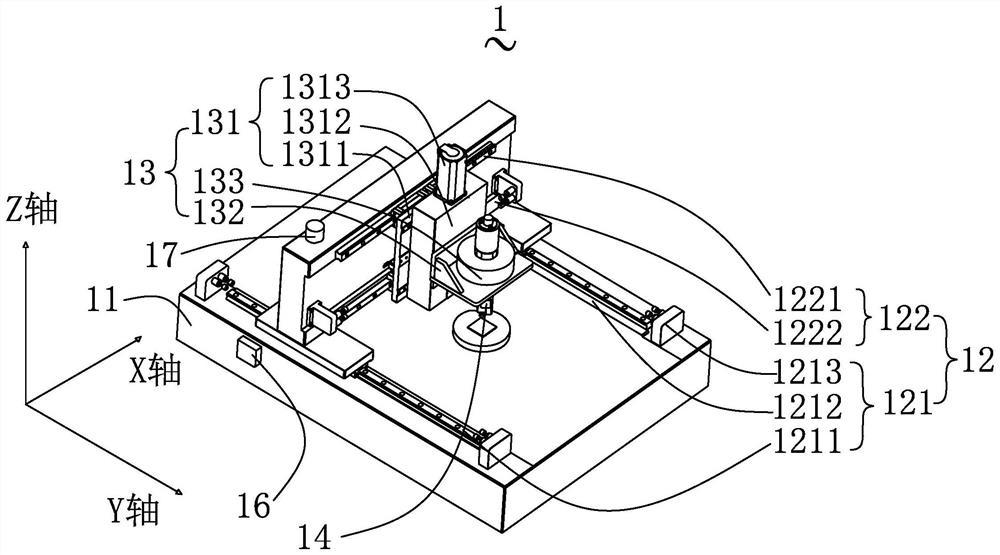
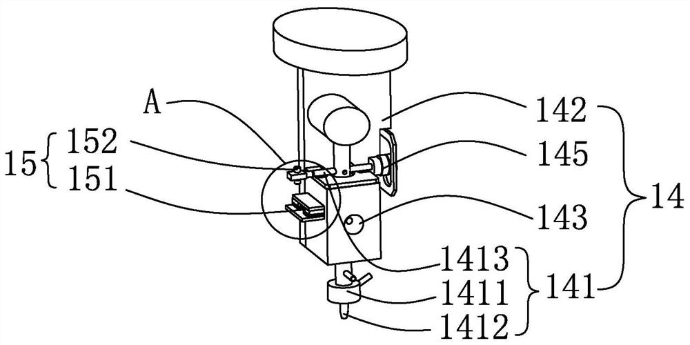
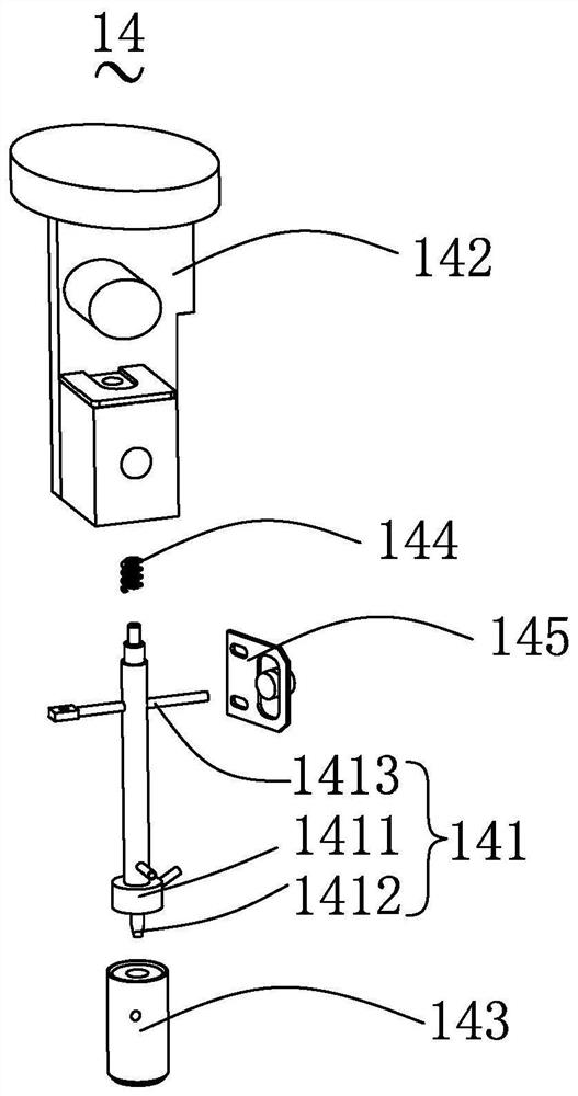
[0035] see figure 1 and figure 2 , the first embodiment of the present invention provides an automatic c...


PUM

PropertyMeasurementUnit
thicknessaaaaaaaaaa
thicknessaaaaaaaaaa

Abstract

The present invention relates to the technical field of chip mounters, in particular to an automatic chip mounter, comprising sequentially connected drive components, die-bonding components, and sensing components. Bonding on the substrate, the sensor component detects the pressure between the chip and the substrate when the chip is bonded by the die-bonding component. During die bonding, the bonding between the wafer and the substrate is not firm or the bonding is dislocated due to too small bonding pressure. At the same time, it can avoid damage to the chip caused by excessive bonding pressure between the chip and the substrate. The pressure when bonding with the substrate is detected, which further improves the installation accuracy between the chip and the substrate when the automatic placement machine solidifies the crystal.

Description

【Technical field】 [0001] The invention relates to the technical field of placement machines, in particular to an automatic placement machine. 【Background technique】 [0002] In the packaging process of electronic equipment, die bonding is one of the most important links. In the early days, mechanical die bonding equipment was usually used to install the chip on the substrate. The placement machine can realize fully automatic and high-speed solid crystal on the substrate; [0003] The commonly used high-speed automatic chip mounter is to pick up and place the chip through the vacuum nozzle. When the vacuum nozzle places the chip on the corresponding position of the substrate, the chip only contacts the substrate by its own gravity, which leads to the chip Due to the weak contact with the substrate, dislocation is prone to occur, which in turn affects the mounting accuracy between the chip and the substrate. At the same time, the above-mentioned automatic placement machine ca...

Claims


Application Information

Patent Timeline
Patent Type & Authority Patents(China)
IPC IPC(8): H01L21/67H01L21/68H01L21/683
CPCH01L21/67121H01L21/6838H01L21/68
Inventor 雷伟庄
Owner 微见智能封装技术(深圳)有限公司
Features
  • R&D
  • Intellectual Property
  • Life Sciences
  • Materials
  • Tech Scout
  • Unparalleled Data Quality
  • Higher Quality Content
  • 60% Fewer Hallucinations
Learn More