Display panel and preparation method of display panel

A technology for display panels and drive backplanes, applied to electrical components, electrical solid-state devices, circuits, etc., can solve problems such as low yield and low transfer rate

Active Publication Date: 2021-04-27
CHENGDU VISTAR OPTEOLECTRONICS CO LTD
View PDF13 Cites 2 Cited by
  • Summary
  • Abstract
  • Description
  • Claims
  • Application Information

AI Technical Summary

Problems solved by technology

[0004] The above-mentioned process of transferring LED chips on the growth s...

Method used


Image

  • Display panel and preparation method of display panel
  • Display panel and preparation method of display panel
  • Display panel and preparation method of display panel

Examples


Embodiment Construction

[0015] The following will clearly and completely describe the technical solutions in the embodiments of the present application with reference to the drawings in the embodiments of the present application. Obviously, the described embodiments are only some of the embodiments of the present application, not all of them. Based on the embodiments in this application, all other embodiments obtained by persons of ordinary skill in the art without making creative efforts belong to the scope of protection of this application.

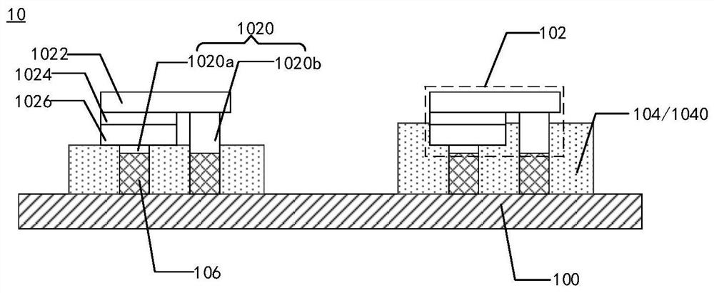
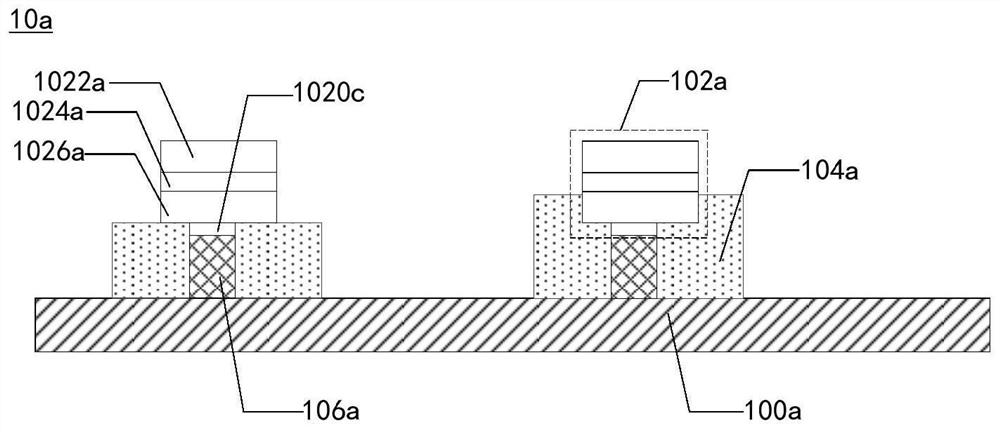
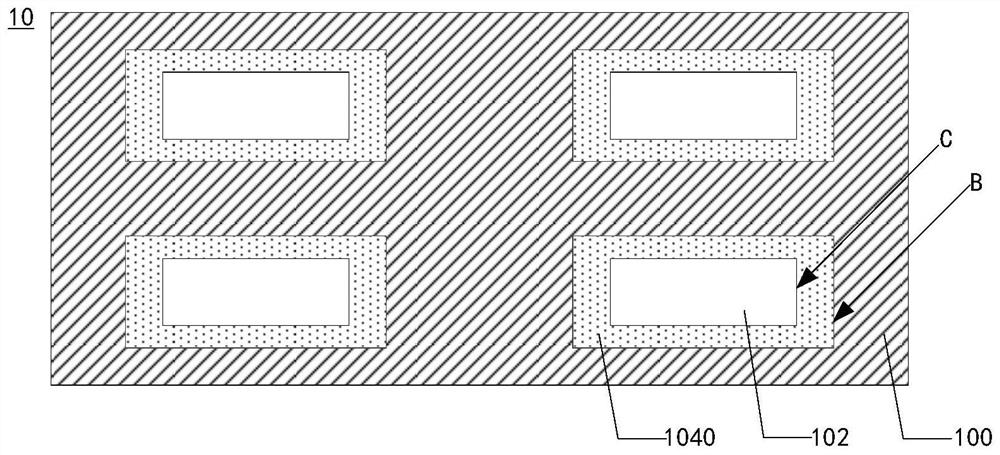
[0016] In the prior art, the specific process of laser lift-off is as follows: first, a plurality of LED chips with a growth substrate are pressed onto a temporary substrate with a temporary bonding glue, so that the multiple LED chips are fixed by the temporary bonding glue; Laser light is then irradiated from the side of the growth substrate to separate the plurality of LED chips from the growth substrate. The specific process of batch transfer is as follows...


PUM


Abstract

The invention discloses a display panel and a preparation method of the display panel. The display panel comprises a driving backboard, a plurality of solder columns and a plurality of LED chips, wherein one side surface of the driving backboard is provided with an adhesive layer, and the adhesive layer is provided with a plurality of through holes arranged in an array; the solder columns are arranged in the through holes, and the solder columns are lower than the through holes; the LED chips are located on the side, provided with the adhesive layer, of the driving backboard, at least one electrode is arranged on one side of each LED chip, and the electrodes are connected with the solder columns. By means of the mode, the risk that the LED chip is broken during laser stripping can be reduced, and the step of picking up the LED chip through a transfer pick-up head in the transfer technology is omitted.

Description

technical field [0001] The present application relates to the field of display technology, in particular to a display panel and a method for preparing the display panel. Background technique [0002] LED (Light Emitting Diode, light-emitting diode) chip display technology has the advantages of high brightness, high response speed, low power consumption, long life, etc., and has become a research hotspot for people to pursue a new generation of display technology. [0003] At present, in the process of manufacturing LED display panels, the LED chips on the growth substrate need to go through two processes of laser lift-off and batch transfer when they are transferred to the driving backplane. [0004] The above-mentioned process of transferring the LED chips on the growth substrate to the driving backplane has the problems of low transfer rate and low yield. Contents of the invention [0005] The present application provides a display panel and a method for preparing the d...

Claims


Application Information

Patent Timeline
IPC IPC(8): H01L27/15H01L33/62H01L33/00
CPCH01L27/156H01L33/62H01L33/0095
Inventor 董小彪曹轩夏继业
Owner CHENGDU VISTAR OPTEOLECTRONICS CO LTD
Why Eureka
Try Eureka