Integrated circuit time delay detection method and device, storage medium and electronic equipment

A technology of integrated circuits and detection methods, applied in the fields of electrical digital data processing, computer-aided design, special data processing applications, etc., can solve problems such as unfavorable efficiency, increase, and increase the burden of simulation process, so as to reduce the number of simulations and improve efficiency. Effect

Pending Publication Date: 2021-05-11
CHENGDU HAIGUANG MICROELECTRONICS TECH CO LTD
View PDF0 Cites 3 Cited by
  • Summary
  • Abstract
  • Description
  • Claims
  • Application Information

AI Technical Summary

Problems solved by technology

However, when the length of the trace changes, it is necessary to simulate the delay again, which increases the burden of the simulation process and is not conducive to the improvement of efficiency.

Method used


Image

  • Integrated circuit time delay detection method and device, storage medium and electronic equipment
  • Integrated circuit time delay detection method and device, storage medium and electronic equipment
  • Integrated circuit time delay detection method and device, storage medium and electronic equipment

Examples


Embodiment Construction

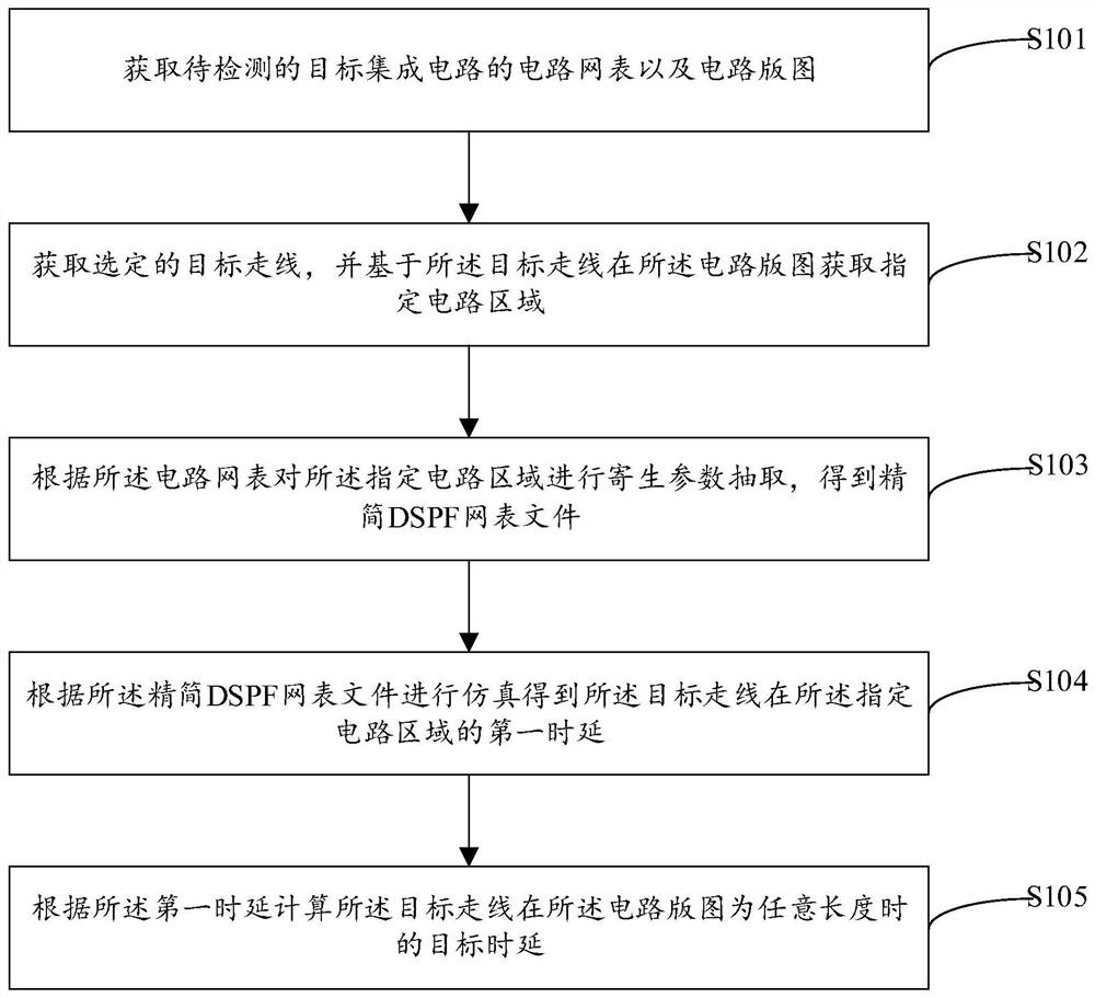
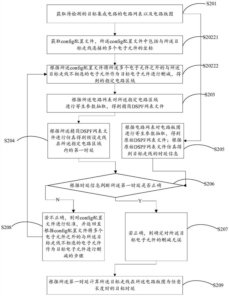
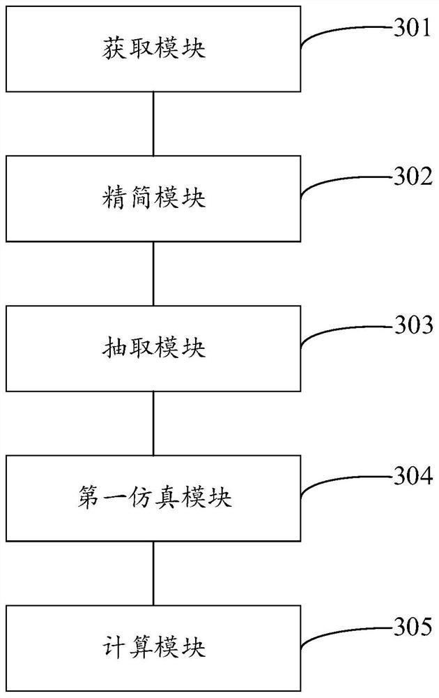
[0051] The technical solutions in the embodiments of the present application will be clearly and completely described below in conjunction with the drawings in the embodiments of the present application.

[0052]In the description of this application, it should be noted that the orientation or positional relationship indicated by the terms "inner", "outer", etc. is based on the orientation or positional relationship shown in the drawings, or the usual placement of the application product when it is used. Orientation or positional relationship is only for the convenience of describing the present application and simplifying the description, and does not indicate or imply that the referred device or element must have a specific orientation, be constructed and operated in a specific orientation, and thus should not be construed as limiting the present application. In addition, the terms "first", "second", etc. are only used for distinguishing descriptions, and should not be constr...


PUM


Abstract

The invention provides an integrated circuit time delay detection method and device, a storage medium and electronic equipment. The integrated circuit time delay detection method comprises the following steps: acquiring a circuit netlist and a circuit layout of a to-be-detected target integrated circuit; acquiring a selected target wire, and acquiring a specified circuit area in the circuit layout based on the target wire; performing parasitic parameter extraction on the specified circuit area according to the circuit netlist to obtain a simplified DSPF netlist file; performing simulation according to the simplified DSPF netlist file to obtain a first time delay of the target wire in the specified circuit area; and according to the first time delay, calculating the target time delay when the target wire is in any length. Therefore, the target time delay of the target wire with any length or after length change can be calculated only through one-time simulation, the simulation frequency can be reduced, and the efficiency can be improved.

Description

technical field [0001] The present application relates to the field of integrated circuit simulation testing, in particular to an integrated circuit delay detection method, device, storage medium and electronic equipment. Background technique [0002] In IC design, there are parasitic parameters that are not required by the design between the interconnection lines, that is, the so-called parasitic parameters. The parasitic parameters include parasitic resistance, capacitance and inductance. In the circuit layout (layout), the distribution of parasitic resistance and parasitic capacitance is complex and dense. As the scale and complexity of circuit layout and layout and routing continue to expand and increase, the parasitic parameter files extracted by EDA tools are also getting larger and larger. In particular, for Memory (memory), there are various repeated units in its circuit layout, and there are many traces and MOS transistors in each unit. If its layout is not simpli...

Claims


Application Information

Patent Timeline
Patent Type & Authority Applications(China)
IPC IPC(8): G06F30/394G06F30/3953
CPCG06F30/394G06F30/3953
Inventor 刘进黄瑞锋赵慧
Owner CHENGDU HAIGUANG MICROELECTRONICS TECH CO LTD
Why Eureka
Try Eureka