Touch sensing module, touch display device and manufacturing method thereof
A touch display device and touch sensing technology, applied in the fields of instruments, computing, electrical and digital data processing, etc., can solve problems such as damage, unusability, and changing the surface resistance value of metal grids, so as to prevent reactions and reduce vulcanization reactions. Effect
- Summary
- Abstract
- Description
- Claims
- Application Information
AI Technical Summary
Problems solved by technology
Method used
Image

Examples
Embodiment Construction
[0035] In order to make the object, technical solution and advantages of the present invention clearer, the present invention will be further described in detail below in conjunction with the accompanying drawings and embodiments. It should be understood that the specific embodiments described here are only used to explain the present invention, but not to limit the present invention.
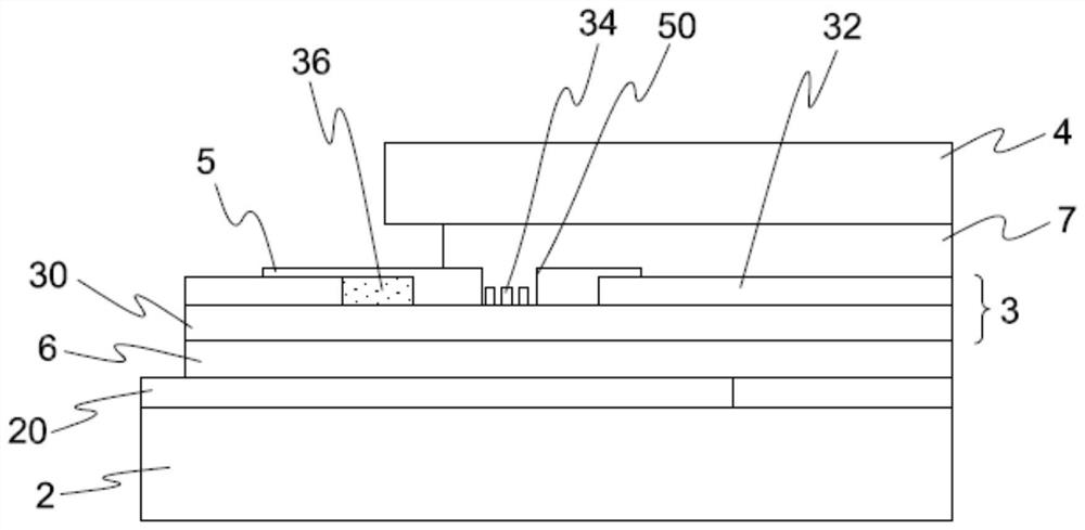
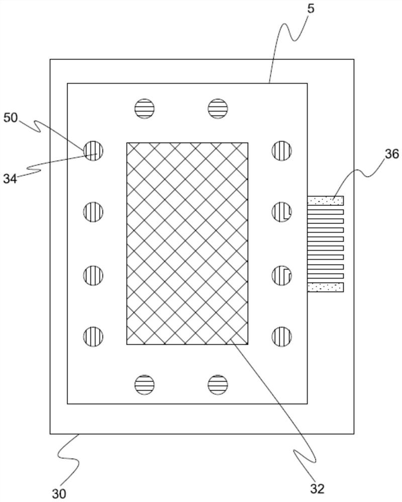
[0036] see figure 2 and image 3As shown, the present invention is a touch display device, including a cover plate 2 (Cover Lens), a touch sensing module 3, a display module 4 (for example: a liquid crystal display module 4), an insulating layer 5, a first connection layer 6 and the second connection layer 7, wherein the first connection layer 6 is disposed between the cover plate 2 and the touch sensing module 3, and the second connection layer 7 is disposed between the touch sensing module 3 and the display module 4 . The first connection layer 6 and the second connection layer 7 are opti...
PUM
| Property | Measurement | Unit |
|---|---|---|
| Width | aaaaa | aaaaa |
| Width | aaaaa | aaaaa |
| Width | aaaaa | aaaaa |
Abstract
Description
Claims
Application Information