

Wafer electroplating device and electroplating method
An electroplating device and wafer technology, applied in the direction of electrodes, circuits, electrolysis process, etc., can solve problems such as uneven thickness of electroplating layer, and achieve the effect of reducing the difficulty of grinding
- Summary
- Abstract
- Description
- Claims
- Application Information
AI Technical Summary
Problems solved by technology
Method used
Image

Examples
Embodiment Construction
[0025] The following will clearly and completely describe the technical solutions in the embodiments of the present invention with reference to the accompanying drawings in the embodiments of the present invention. Obviously, the described embodiments are only some, not all, embodiments of the present invention. Based on the embodiments of the present invention, all other embodiments obtained by persons of ordinary skill in the art without creative efforts fall within the protection scope of the present invention.
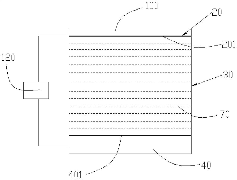
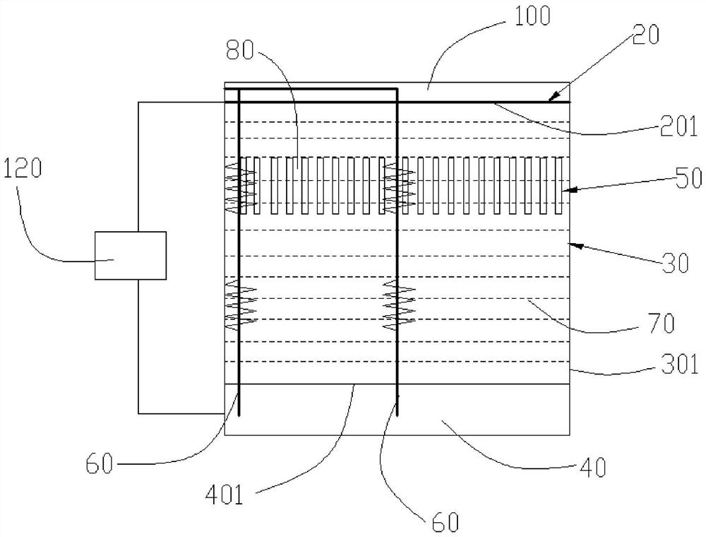
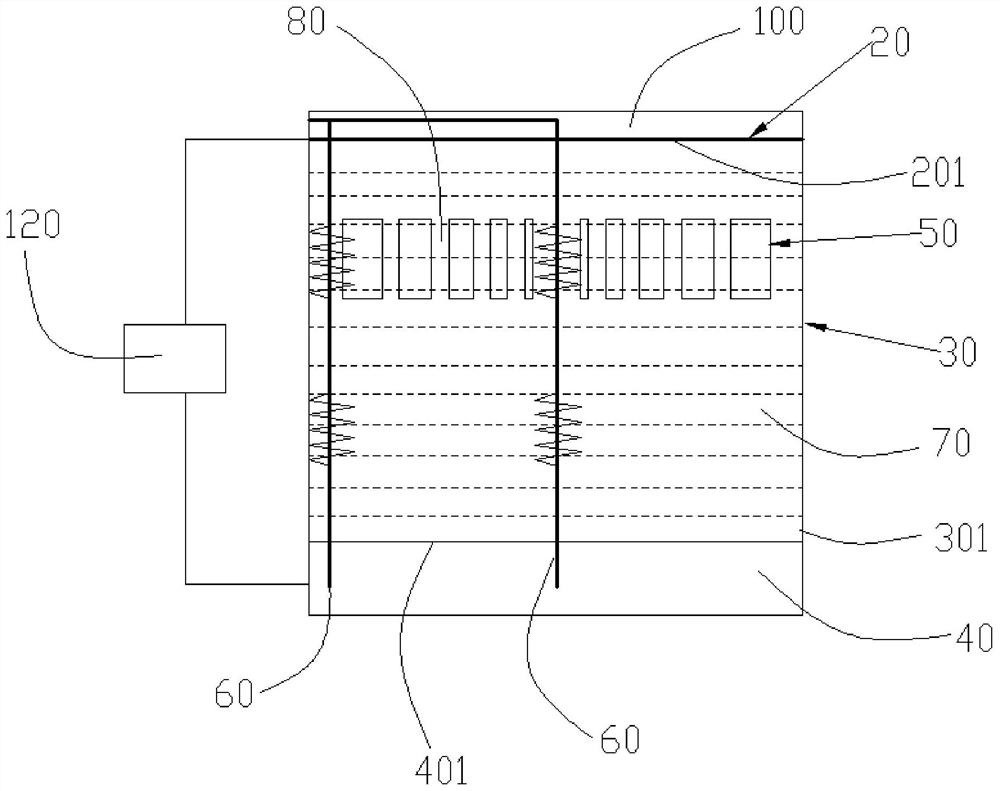
[0026] Before describing the embodiments of the present invention, a conventional wafer 100 plating apparatus will be described first.
[0027] see figure 1 , the electroplating device of traditional wafer 100 comprises electroplating tank 30, electroplating anode 40 and power supply 120, is provided with electroplating solution 70 in electroplating tank 30, and the surface of wafer 100 is provided with seed layer 20, and electroplating anode 40 includes towards se...
PUM
 Abstract
Description
Claims
Application Information