A Pixel Circuit and Thin Film Transistor Backplane Compensating for Threshold Voltage Shift

A technology for voltage drift and threshold compensation. It is used in static indicators, instruments, etc., and can solve problems such as uneven current and uneven image display.

Active Publication Date: 2015-10-14
BOE TECH GRP CO LTD
View PDF11 Cites 0 Cited by
  • Summary
  • Abstract
  • Description
  • Claims
  • Application Information

AI Technical Summary

Problems solved by technology

[0004] An embodiment of the present invention provides a pixel circuit and a thin film transistor backplane for compensating for threshold voltage drift, so as to solve the problems caused by the threshold voltage drift of the existing backplane thin film transistors that flow through different OLEDs when the same image frame data signal is received. The uneven current causes the problem of uneven display of the entire image

Method used


Image

  • A Pixel Circuit and Thin Film Transistor Backplane Compensating for Threshold Voltage Shift
  • A Pixel Circuit and Thin Film Transistor Backplane Compensating for Threshold Voltage Shift
  • A Pixel Circuit and Thin Film Transistor Backplane Compensating for Threshold Voltage Shift

Examples


Embodiment Construction

[0021] The specific implementation manners of a pixel circuit for compensating threshold voltage drift and a thin film transistor backplane provided by an embodiment of the present invention will be described below with reference to the accompanying drawings.

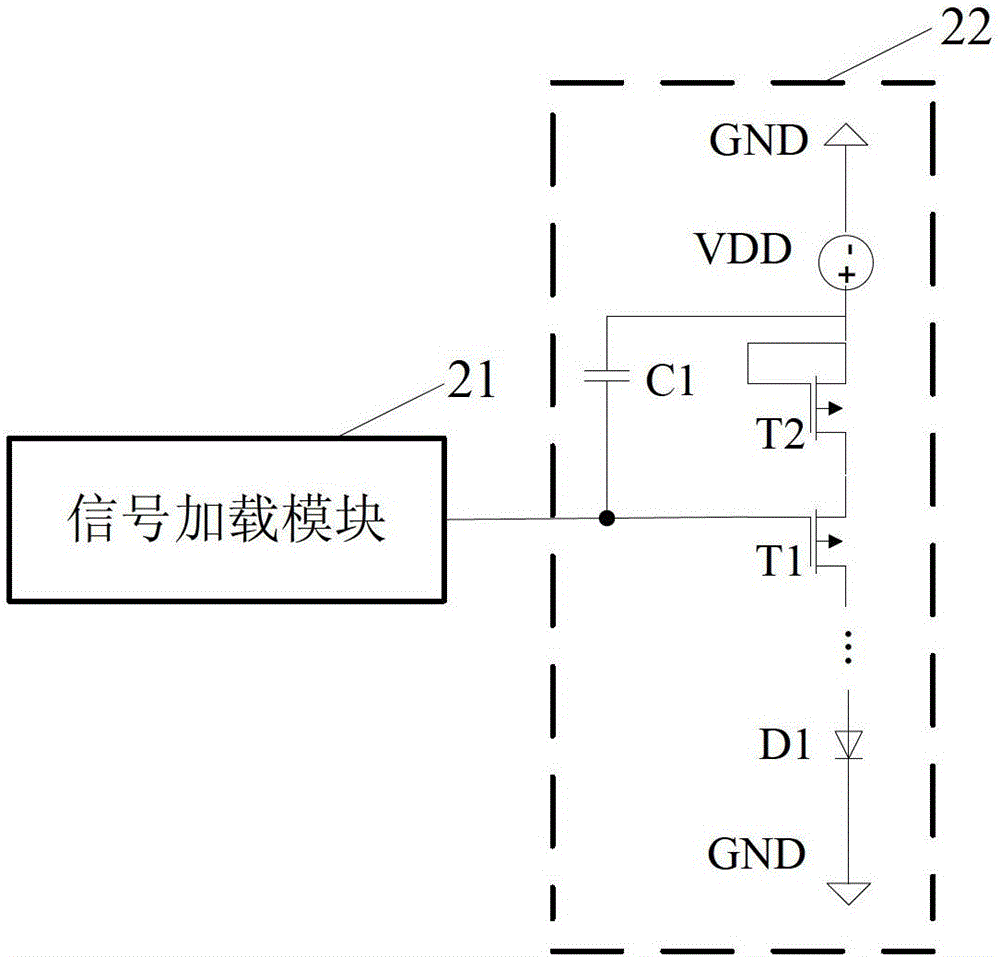
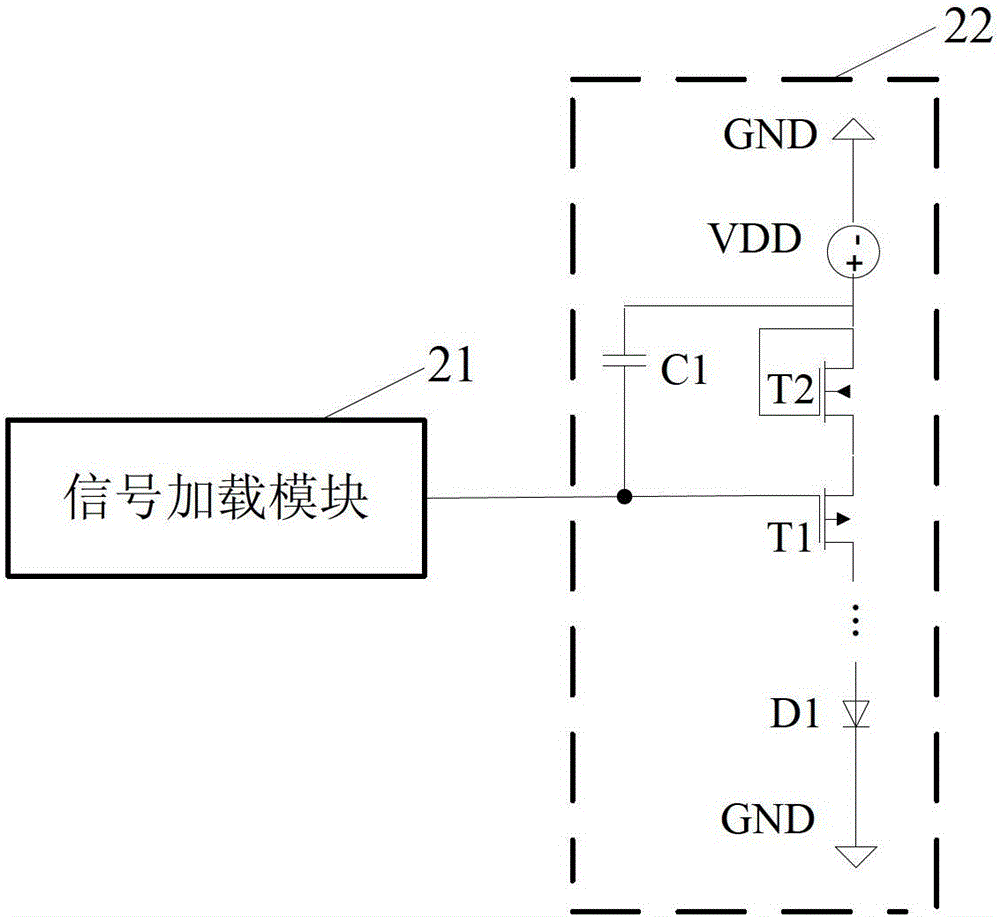
[0022] A pixel circuit for compensating threshold voltage drift provided by the embodiment of the present invention has two implementation methods, the first one is as Figure 2a As shown, the structure of the pixel circuit specifically includes:

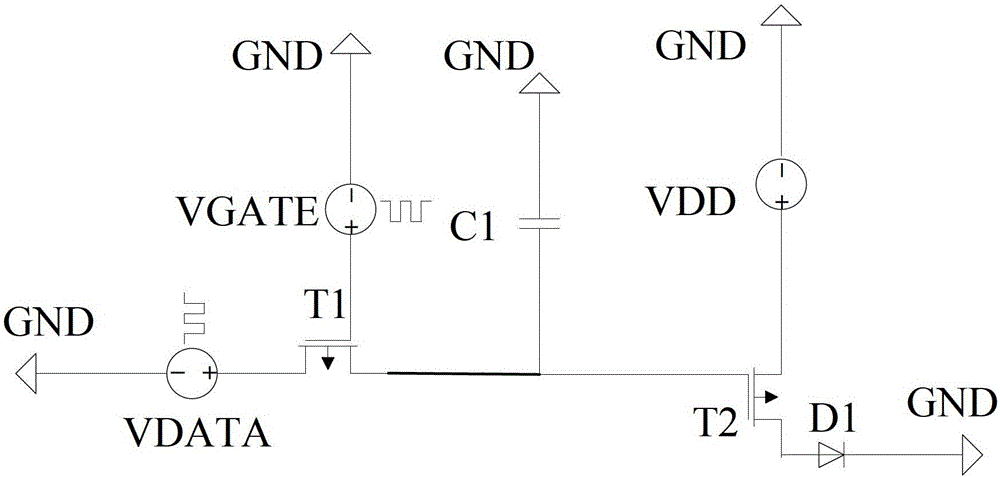
[0023] A signal loading module 21 and a driving module 22, wherein the signal loading module 21 is used to output the current frame data signal, and the driving module 22 includes a VDD signal source, a driving transistor T1, a storage capacitor C1, a p-type decay transistor T2 and an OLED D1, wherein, p The drain of the p-type attenuation transistor T2 is connected to the source of the drive transistor T1, the gate of the p-type attenuation transistor T2 is connected to the ...


PUM


Abstract

The embodiment of the invention provides a pixel circuit for compensating shift of a threshold voltage and a thin film transistor backplane, so as to solve the problem of uneven display of an image caused by the shift of the threshold voltage in the prior art. The pixel circuit comprises a driver module and a signal loading module, wherein the driver module comprises a VDD (virtual device driver) signal source, a driver transistor T1, a storage capacitance C1 and an OLED (organic light emitting diode) D1; a grid electrode of the driver transistor T1 is connected with an output end of the signal loading module and drives the OLED D1 to emit light; one end of the storage capacitance C1 is connected with an output end of the VDD signal source, and the other end of the storage capacitance C1 is connected with the grid electrode of the driver transistor T1; the driver module further comprises a p-shaped decaying transistor T2, the grid electrode is connected with a source electrode and is connected with the output end of the VDD signal source, a drain electrode is connected with the source electrode of the driver transistor T1; alternatively, the driver module further comprises a n-shaped decaying transistor T2, the grid electrode is connected with the drain electrode and is connected with the output end of the VDD signal source, and the source electrode is connected with that of the driver transistor T1.

Description

technical field [0001] The invention relates to the technical field of liquid crystal display, in particular to a pixel circuit and a thin film transistor backplane for compensating threshold voltage drift. Background technique [0002] Active Matrix Organic Light Emitting Diode (AMOLED) displays have been widely used due to their advantages of wide viewing angle, good color contrast effect, fast response speed and low cost. However, due to the non-uniformity and stability problems of the thin film transistor (Thin Film Transistor, TFT) backplane in the process, the threshold voltage will drift. [0003] The traditional 2T1C pixel circuit such as figure 1 As shown, it includes: gate signal source VGATE, image frame data signal source VDATA, VDD signal source, switching transistor T1, driving transistor T2, storage capacitor C1 and organic light emitting diode (Organic Light Emitting Diode, OLED) D1, etc., wherein the switching transistor The gate of T1 is connected to the ...

Claims


Application Information

Patent Timeline
Patent Type & Authority Patents(China)
IPC IPC(8): G09G3/32G09G3/3233
Inventor 马占洁
Owner BOE TECH GRP CO LTD
Why Eureka
Try Eureka