Optical modulating/display device and production method therefor and display apparatus mounting the optical modulating/displaying device thereon

Inactive Publication Date: 2005-07-07
NEC CORP
View PDF13 Cites 62 Cited by
  • Summary
  • Abstract
  • Description
  • Claims
  • Application Information

AI Technical Summary

Benefits of technology

[0009] An object of the present invention is to provide an optical modulating displ

Problems solved by technology

The reflective liquid crystal displaying device, however, uses an ambient external light, therefore when ambient light is poor like in night time, display is not easy to be seen or cannot be seen.
However, if a liquid crystal displaying device is provided with a front light on the outside thereof, a depth feel corresponding to thickness of the front light occurs on a display, thereby resulting in deterioration in quality level of display.
Thus, light guiding may not be sufficiently performed up to an opposite side face to the light incoming side which is a side face opposite to the side face of the transparent substrate into which the light enters.
Consequently, non-uniformity in display illumination is caused in a display surface.
Similar to the first prior art, however, refractive index of PVA (polyvinyl alcohol) which is generally used as a main component of t

Method used


Image

  • Optical modulating/display device and production method therefor and display apparatus mounting the optical modulating/displaying device thereon
  • Optical modulating/display device and production method therefor and display apparatus mounting the optical modulating/displaying device thereon
  • Optical modulating/display device and production method therefor and display apparatus mounting the optical modulating/displaying device thereon

Examples


first embodiment

[0148] Embodiments of the present invention will be described below in reference to accompanied drawings in order to make clear objects, features and advantages of the present invention.

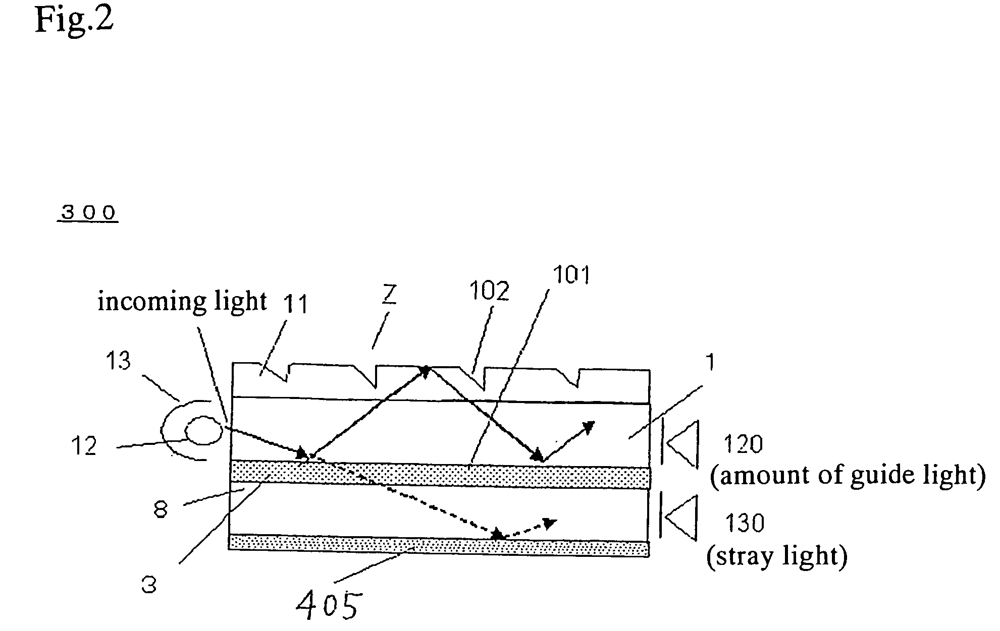
[0149]FIG. 6 is a cross-sectional view of an optical modulating display device according to first embodiment of the present invention. In the present embodiment, an optical modulating layer is constituted of a layer filled with charged fine particles. The optical modulating device in the present embodiment includes a pair of first substrate 400 and second substrate 401, a multilayer structure sandwiched between the first and second substrates 400 and 401. The multilayer structure has a structure in which a low refraction layer 402 being lower in refractive index than the first substrate 400, a first transparent electrode layer 3-1 for applying voltage, a first insulating layer 403-1, a charged fine particle filled layer 404 filled with the charged fine particle, a second insulating layer 403-2, and ...

second embodiment

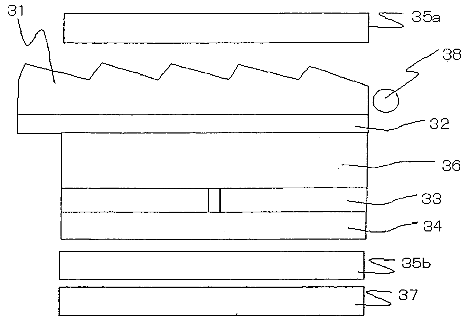
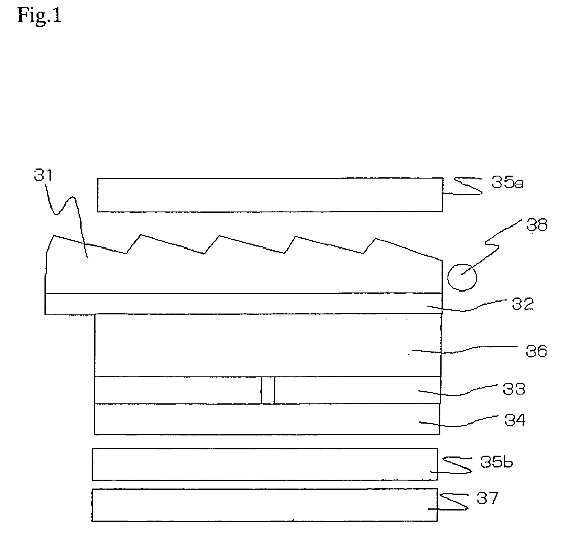
[0173]FIG. 8 is a cross-sectional view of an optical modulating display device according to second embodiment of the present invention. A liquid crystal displaying device in the present embodiment includes a multilayer structure containing a liquid crystal layer and a pair of first substrate 1 and second substrate 2 comprising transparent substrates sandwiching the multilayer structure. The multilayer structure is constituted of a laminated structure comprising, viewed from an observer's side, namely from an upper part of the drawing, a low refraction layer 3 being lower in refractive index than the transparent substrate and comprising a transparent material layer, a color filter layer 4 for color displaying, a polarizing layer 5 for transmitting only specific polarized light component, a phase difference layer 6 comprising at least one layer for performing an optical compensation of liquid crystal, a transparent electrode layer 7 for applying voltage thereon, a liquid crystal layer...

third embodiment

[0194] Then, a preparing method of the present embodiment will be specifically described below.

[0195]FIG. 10A to 10G are cross-sectional views illustrating a production method of an optical modulating (liquid crystal) displaying device in an embodiment according to the present invention, where FIG. 10A to 10C show manufacturing processes of a first glass substrate in a liquid crystal displaying device combining a light guiding function of a front light and FIG. 10D to 10F show manufacturing processes of a second glass substrate and assembling processes of a liquid crystal displaying portion. FIG. 10G also shows a manufacturing process of a protruded portion in the liquid crystal displaying device in the present invention. As a flow of schematic processes of production, the liquid crystal displaying portion 14 is first prepared and the protruded portion 11 is then formed on the liquid crystal displaying portion 14.

[0196] As illustrated in FIG. 10A, after uniformly applying a UV cur...


PUM


Abstract

The present invention relates to an optical modulating display device (200) such as a liquid crystal displaying device provided with a front-light type planar illuminating device.
The above front-light type planar illuminating device allows illuminating light to propagate inside a substrate (1), and is provided with a low refraction layer (3) being lower in refractive index than the substrate (1) and being in close contact with the inner surface of the substrate (1), and with reflection structure (11) on the outer surface of the substrate (1).
The optical modulating display device (200) provided with the above front-light type planar illuminating device can ensure a sufficient amount of guide light propagating inside the substrate (1) and reduce non-uniformity in display illumination.
And a display apparatus mounting the above optical modulating display device (200) thereon can be reduced in thickness and weight and provide a high quality display.

Description

TECHNICAL FIELD [0001] The present invention relates to an optical modulating display device provided with a planar illuminating system for illuminating a displaying device, a production method therefor and a display apparatus mounting the optical modulating display device thereon. BACKGROUND OF THE ART [0002] A reflective liquid crystal displaying device is widely used for a display of an electronic apparatus such as a cellular phone and a personal digital assistant of which a main power supply is a battery. The reflective liquid crystal displaying device, however, uses an ambient external light, therefore when ambient light is poor like in night time, display is not easy to be seen or cannot be seen. Consequently, in these years, the reflective liquid crystal displaying device is provided with a front light for illuminating from an observer's side, whereby the front light is put the light on in order to make it easy to see the display even in an environment such as in the dark whe...

Claims


Application Information

Patent Timeline
IPC IPC(8): F21V8/00G02F1/1335G02F1/13357
CPCG02B6/0053G02F2001/133616G02F1/133615G02F1/133605G02F1/133616
Inventor MIMURA, KOJISUMIYOSHI, KENSAITOH, GOROHMATSUSIMA, JINYAGI, YOSHIE
Owner NEC CORP
Why Eureka
Try Eureka