Etching solution for multilayer thin film having copper layer and molybdenum layer contained therein

A multi-layer thin film and etching solution technology, which is applied to electrical components, circuits, and electric solid-state devices, etc., can solve the problem that it cannot fully cope with the large-scale and high-resolution displays, the cross-sectional shape of the wiring cannot be fully satisfied, and the environmental measures cannot be fully satisfied. and other problems, to achieve the effect of prolonging the life of the plating solution, good wiring cross-section shape, and less unevenness

Active Publication Date: 2012-10-31
MITSUBISHI GAS CHEM CO INC
View PDF7 Cites 62 Cited by
  • Summary
  • Abstract
  • Description
  • Claims
  • Application Information

AI Technical Summary

Problems solved by technology

However, although copper has the advantage of low resistance, on the other hand, it has the following problems: when it is used for gate wiring (gate wiring), the adhesion between substrates such as glass and copper is not sufficient, and in the source / When used for drain wiring, diffusion may occur in the underlying organic silicon semiconductor film
[0006] However, the cross-sectional shape of the wiring after etching is not sufficient, and as a result, it may not be able to fully cope with the increase in size and resolution of the display.
In addition, the etching solution disclosed in Patent Document 2 contains a fluorinated compound, which is not sufficiently satisfactory from the viewpoint of environmental measures.

Method used


Image

  • Etching solution for multilayer thin film having copper layer and molybdenum layer contained therein
  • Etching solution for multilayer thin film having copper layer and molybdenum layer contained therein
  • Etching solution for multilayer thin film having copper layer and molybdenum layer contained therein

Examples


Embodiment 1~5

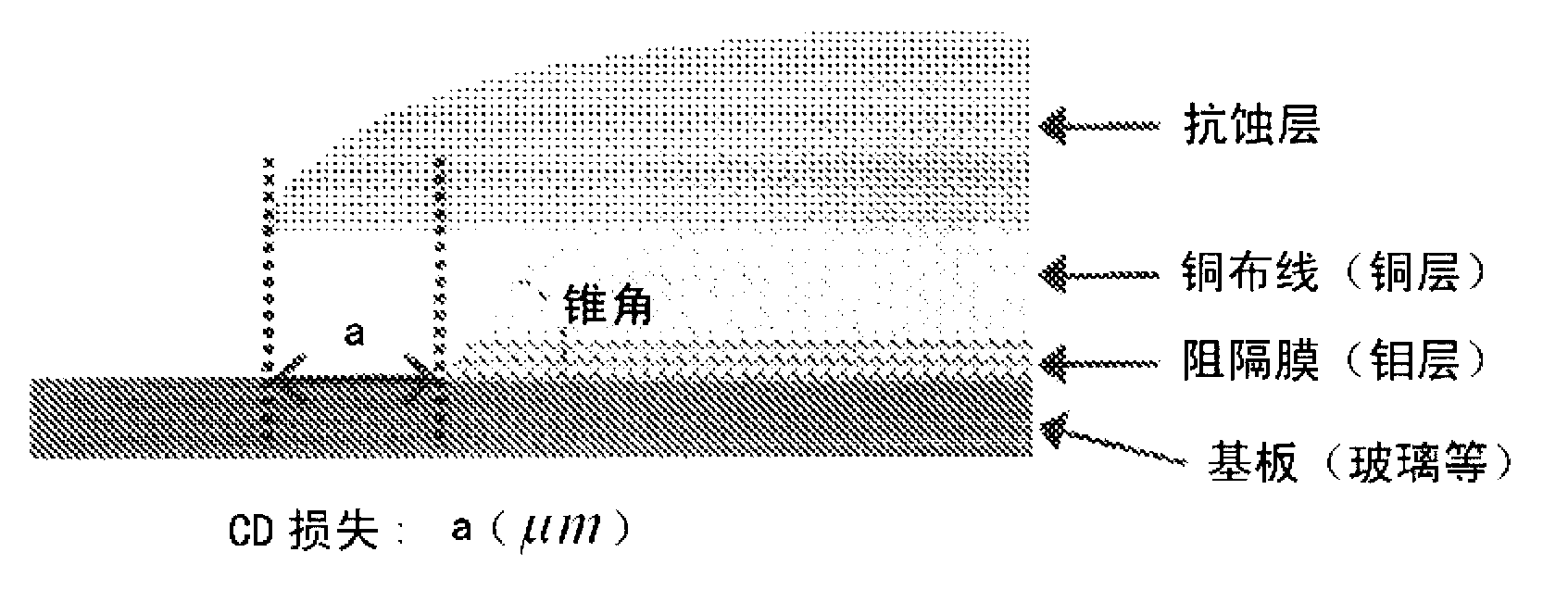
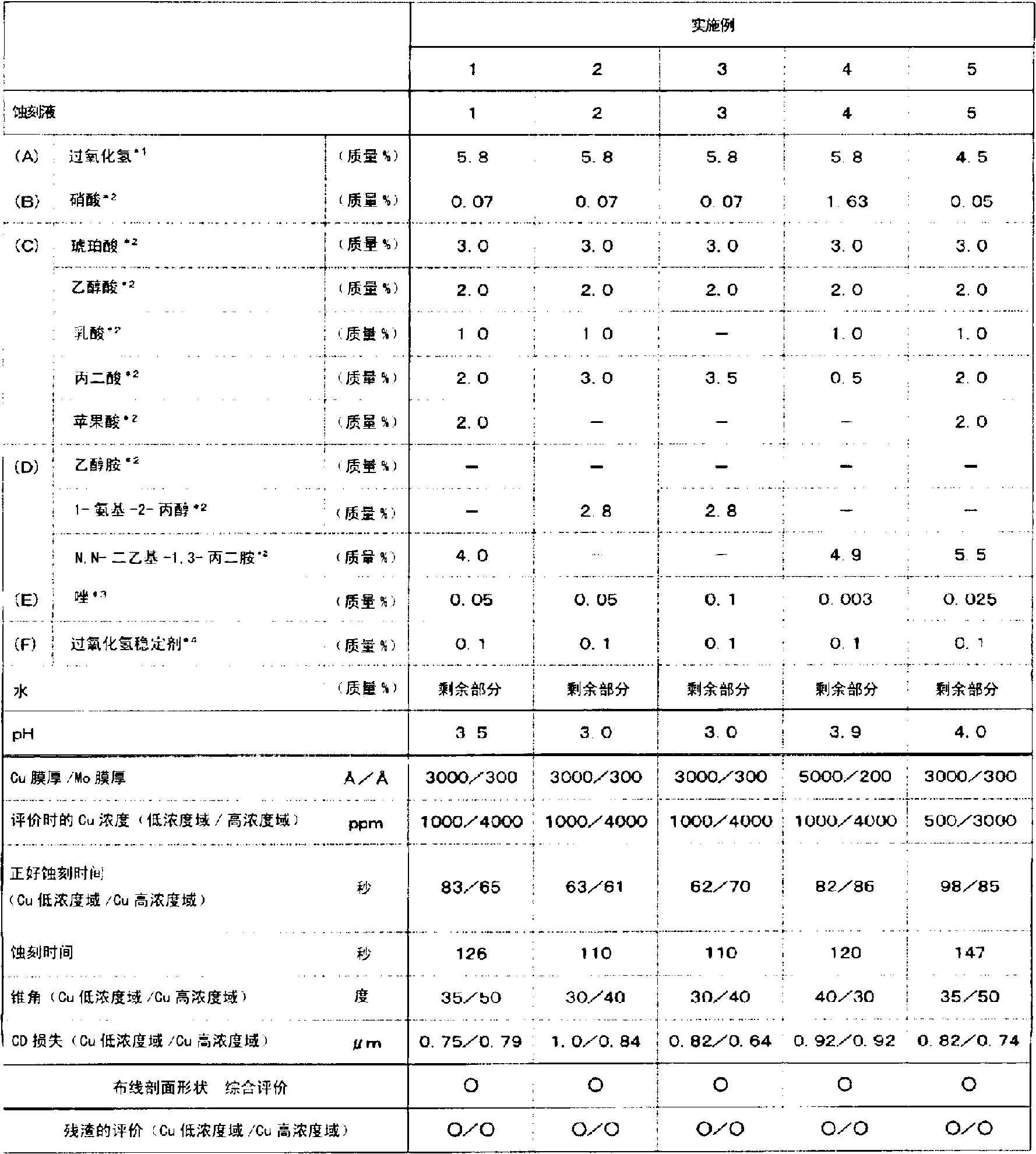
[0084] The multilayer film comprising copper layer and molybdenum layer obtained by the production example is shower sprayed in the etchant shown in Table 2, and the operation of etching is repeated at 35 ° C. For the resulting etched copper layer and molybdenum layer The multi-layer thin film sample of the above-mentioned method is observed by SEM to obtain that the copper ion concentration (sometimes recorded as Cu concentration) in the etching solution is in the low concentration range (200-1000ppm, sometimes recorded as Cu low concentration range) and in the high Cone angle, CD loss (μm) in concentration range (3000-4000ppm, sometimes recorded as Cu high concentration range).

[0085] In addition, the time when the object to be etched in the region where the resist is not patterned is visually judged is etched is set as just etching time (just etching time), and any time within the range of 110 to 300% of the just etching time The time for performing the etching process (o...

Embodiment 6 and 7

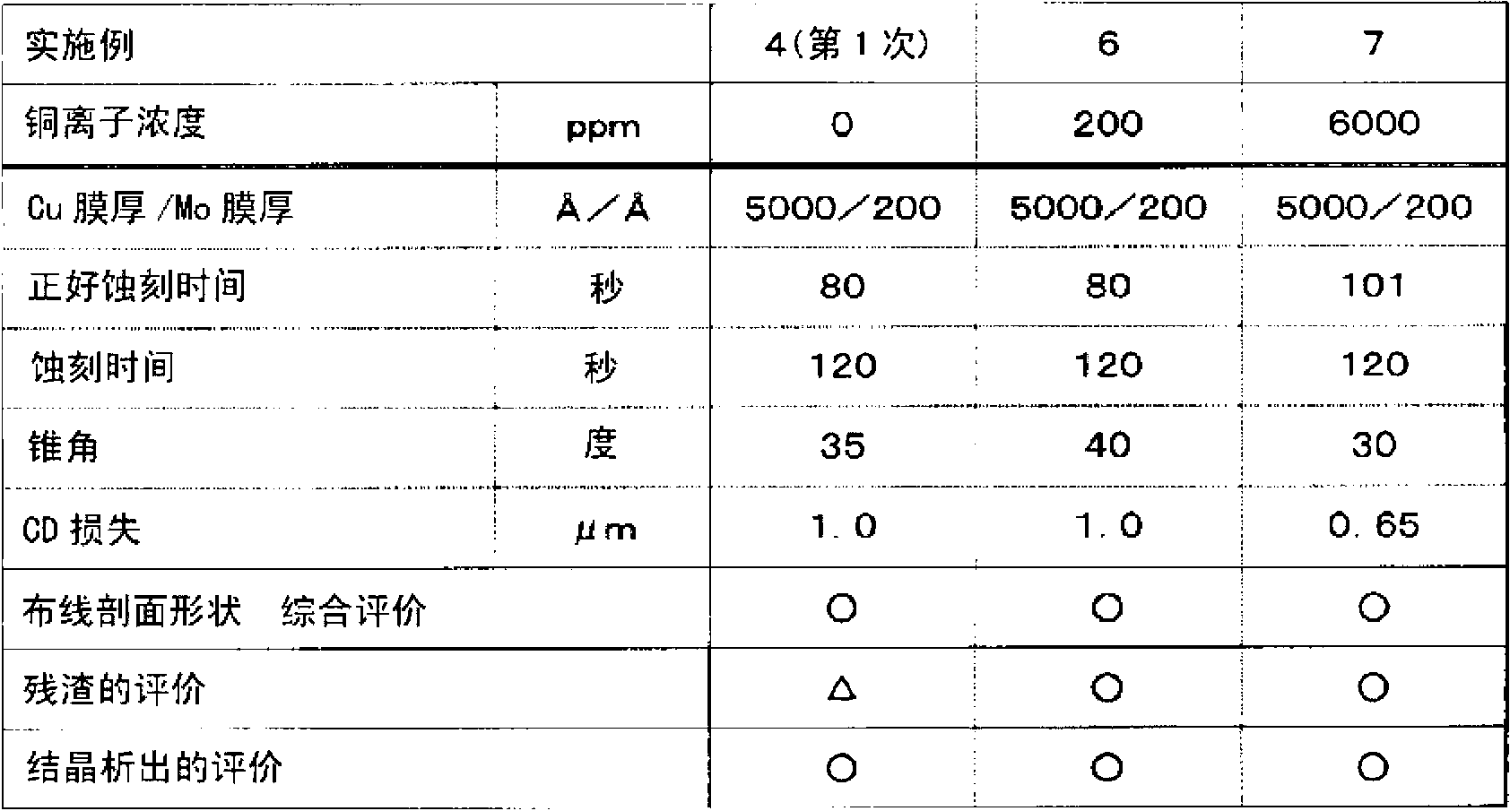
[0093] Except having previously added copper powder to the etching solution 4 used in Example 4 so that the copper ion concentration may be 200ppm and 6000ppm, it carried out similarly to Example 4, and etched, respectively, as Examples 6 and 7. Table 3 shows the evaluation of the taper angle, CD loss (μm), and residue of the multilayer thin film including the copper layer and the molybdenum layer obtained by performing the first etching. In addition, Table 3 shows the evaluation of the taper angle, CD loss (μm), and residue of the multilayer thin film including the copper layer and the molybdenum layer obtained by performing the first etching in Example 4.

[0094] [table 3]

[0095]


PUM


Abstract

Disclosed are: an etching solution for a multilayer thin film having a copper layer and a molybdenum layer contained therein; and a method for etching a multilayer thin film having a copper layer and a molybdenum layer contained therein using the etching solution. Specifically disclosed are: an etching solution for a multilayer thin film having a copper layer and a molybdenum layer contained therein, which comprises (A) hydrogen peroxide, (B) an inorganic acid having no fluorine atom, (C) an organic acid, (D) an amine compound having 2 to 10 carbon atoms and also having an amino group and a hydroxy group in the total number of two or more, (E) an azole, and (F) a hydrogen peroxide stabilizer, and which has a pH value of 2.5 to 5; and an etching method using the etching solution.

Description

technical field [0001] The invention relates to an etchant for a multilayer thin film including a copper layer and a molybdenum layer. In particular, the etchant of the present invention is suitably used for etching a multilayer thin film in which a copper layer is provided on a molybdenum layer. Background technique [0002] Conventionally, aluminum or aluminum alloys have generally been used as wiring materials for display devices such as flat panel displays. However, with the increase in size and resolution of displays, such an aluminum-based wiring material tends to cause a problem of signal delay due to characteristics such as wiring resistance, and it tends to be difficult to perform uniform screen display. [0003] Therefore, studies to use copper as a material with lower resistance or wirings mainly composed of copper are underway. However, although copper has the advantage of low resistance, on the other hand, it has the following problems: when it is used for gat...

Claims


Application Information

Patent Timeline
Patent Type & Authority Applications(China)
IPC IPC(8): C23F1/18C23F1/30H01L21/308H01L21/3205H01L21/3213H01L23/52
CPCH01L21/32134H01L23/53238C23F1/18C23F1/44C23F1/26H01L2924/0002H01L2924/00C23F1/30H01L21/308H01L21/3205
Inventor 冈部哲成田和代松原将英安谷屋智幸丸山岳人
Owner MITSUBISHI GAS CHEM CO INC
Why Eureka
Try Eureka