Light emitting device
A technology of light-emitting devices and light-emitting units, applied in the optical field, can solve problems such as human eye irritation, and achieve the effects of reducing the degree of irritation, improving the service life, and improving the light output efficiency.
- Summary
- Abstract
- Description
- Claims
- Application Information
AI Technical Summary
Problems solved by technology
Method used
Image

Examples
Embodiment 1
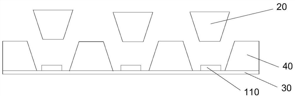
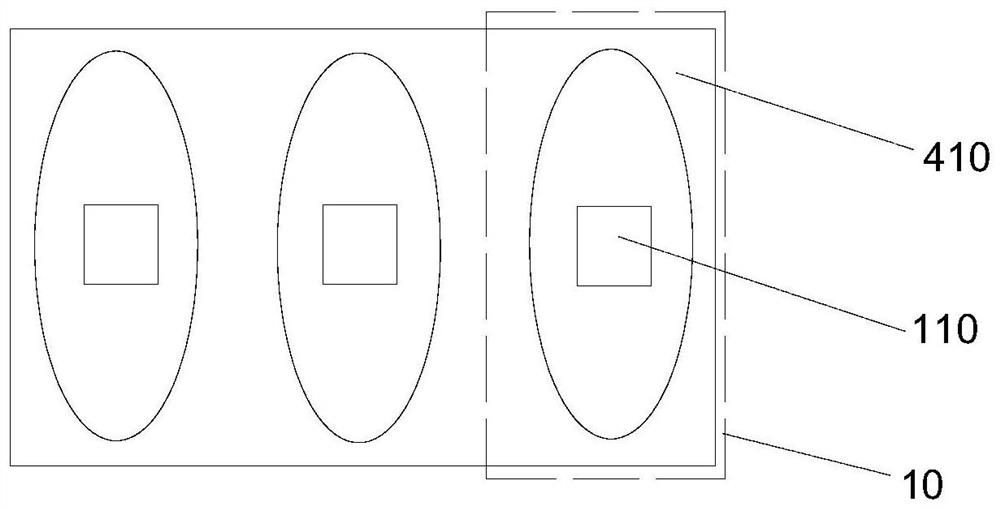
[0042] The 6-inch light-emitting device provided by this embodiment is as figure 1 As shown, it includes a substrate layer 30, a pixel isolation structure 40, at least one light-emitting unit 10, and a light diffusion structure 20. The pixel isolation structure 40 is disposed on one side surface of the substrate layer 30, and multiple mutually isolated pixel structures are formed in the pixel isolation structure 40. The pixel isolation structure is composed of a plurality of isolation units 410 connected, and each isolation unit 410 surrounds the sub-pixel area in one-to-one correspondence; each light emitting unit 10 is composed of a blue QLED light emitting unit 110 and a non-light emitting area, and each light emitting unit The light-emitting units 110 in Figure 10 are arranged in a one-to-one correspondence in the sub-pixel area, and the area other than the light-emitting unit 110 in the sub-pixel area and the isolation unit 410 constitute a non-light-emitting area, definin...
Embodiment 2
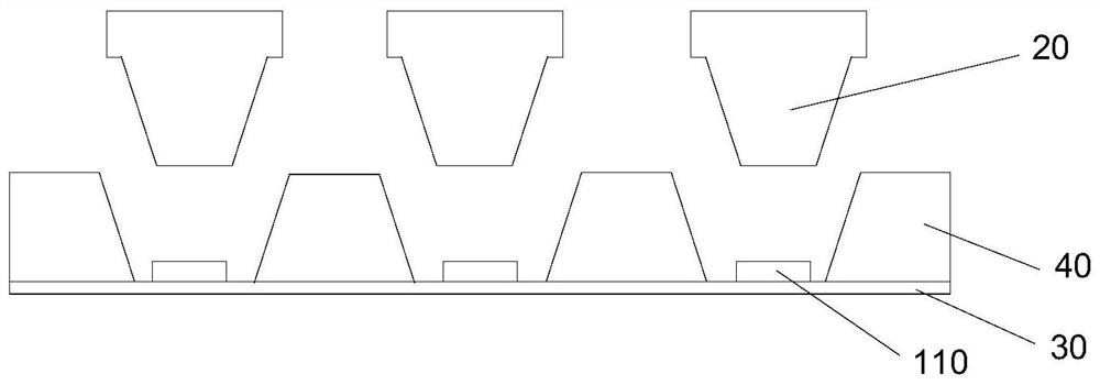
[0046] The 6-inch light-emitting device provided by this embodiment is as image 3 As shown, it includes a substrate layer 30, a pixel isolation structure 40, at least one light-emitting unit 10, and a light diffusion structure 20. The pixel isolation structure 40 is disposed on one side surface of the substrate layer 30, and multiple mutually isolated pixel structures are formed in the pixel isolation structure 40. The pixel isolation structure is composed of a plurality of isolation units 410 connected, and each isolation unit 410 surrounds the sub-pixel area in one-to-one correspondence; each light emitting unit 10 is composed of a blue QLED light emitting unit 110 and a non-light emitting area, and each light emitting unit The light-emitting units 110 in Figure 10 are arranged in a one-to-one correspondence in the sub-pixel area, and the area other than the light-emitting unit 110 in the sub-pixel area and the isolation unit 410 constitute a non-light-emitting area, definin...
Embodiment 3
[0050] The 6-inch light-emitting device provided by this embodiment is as Figure 4As shown, it includes a substrate layer 30, a pixel isolation structure 40, at least one light-emitting unit 10, and a light diffusion structure 20. The pixel isolation structure 40 is disposed on one side surface of the substrate layer 30, and multiple mutually isolated pixel structures are formed in the pixel isolation structure 40. The pixel isolation structure is composed of a plurality of isolation units 410 connected, and each isolation unit 410 surrounds the sub-pixel area in one-to-one correspondence; each light emitting unit 10 is composed of a blue QLED light emitting unit 110 and a non-light emitting area, and each light emitting unit The light-emitting units 110 in Figure 10 are arranged in a one-to-one correspondence in the sub-pixel area, and the area other than the light-emitting unit 110 in the sub-pixel area and the isolation unit 410 constitute a non-light-emitting area, definin...
PUM
| Property | Measurement | Unit |
|---|---|---|
| Width | aaaaa | aaaaa |
| Length | aaaaa | aaaaa |
| Length | aaaaa | aaaaa |
Abstract
Description
Claims
Application Information
 - Generate Ideas
- Intellectual Property
- Life Sciences
- Materials
- Tech Scout
- Unparalleled Data Quality
- Higher Quality Content
- 60% Fewer Hallucinations
Browse by: Latest US Patents, China's latest patents, Technical Efficacy Thesaurus, Application Domain, Technology Topic, Popular Technical Reports.
© 2025 PatSnap. All rights reserved.Legal|Privacy policy|Modern Slavery Act Transparency Statement|Sitemap|About US| Contact US: help@patsnap.com