Supercharge Your Innovation With Domain-Expert AI Agents!

Device and method for suppressing defects in optical components

A technology for optical components and equipment, applied in chemical instruments and methods, cleaning methods using gas flow, cleaning methods and utensils, etc., can solve problems such as affecting components, surface contamination, and reducing component surface accuracy.

Active Publication Date: 2022-05-03
LASER FUSION RES CENT CHINA ACAD OF ENG PHYSICS
View PDF0 Cites 0 Cited by
  • Summary
  • Abstract
  • Description
  • Claims
  • Application Information

AI Technical Summary

Problems solved by technology

[0002] Since the optical element is easily deformed when the side is stressed, it will reduce the surface shape accuracy of the processed element. Introduce surface contamination, which will affect the quality of clamping and adsorption at the edge
At present, the commonly used clamping method is adsorption clamping. During the process of adsorption and clamping, tiny particles such as dust and chips in the processing environment will be introduced between the optical element and the surface of the adsorption fixture, and the particles will be embedded in the optical element after being pressed in the interface. When the clamping surface is mounted, a brittle indentation will be formed, or scratches will be drawn on the clamping surface of the optical element, which will directly affect the damage characteristics of the element and shorten the service life of the optical element
Therefore, there is a technical problem that optical components are prone to surface defects during the adsorption and clamping process

Method used


Image

  • Device and method for suppressing defects in optical components
  • Device and method for suppressing defects in optical components
  • Device and method for suppressing defects in optical components

Examples


Embodiment Construction

[0043] The technical solutions in the embodiments of the present application will be described below with reference to the accompanying drawings in the embodiments of the present application.

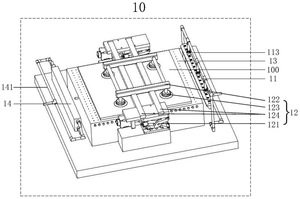
[0044] figure 1 For the structural diagram of an optical element defect suppression device provided in the embodiment of this application, please refer to figure 1 , the suppression device 10 of the optical element defect may include:

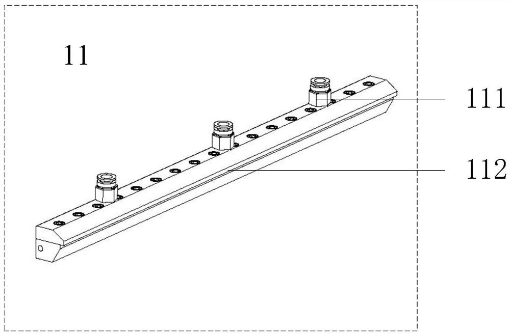
[0045]Purging device 11, adsorption device 12, first suction cup 13 and clean container, described adsorption device 12, described purging device 11 and described first suction cup 13 are all installed in the described clean container; The air outlet of 11 faces the surface to be cleaned of the optical element 100; the adsorption device 12 includes a suction lifting mechanism 121 and an adsorption mechanism, and the suction lifting mechanism 121 is connected with the adsorption mechanism; the first suction cup 13 is arranged on On the base of the clean...


PUM


Abstract

The present application provides a device and method for suppressing defects in optical components. The device for suppressing defects in optical components includes: a purging device, an adsorption device, a first suction cup, and a clean container. The adsorption device, the purging device and the first suction cup are both Installed in a clean container; the air outlet of the purging device faces the surface to be purged of the optical element; the first suction cup is arranged on the base of the clean container, and the first suction cup is arranged opposite to the adsorption mechanism; the adsorption device is used to absorb the optical element The adsorption surface is driven by the lifting mechanism to adjust the optical element to the purge height; the purge device is used to purge the surface to be purged of the optical element; the adsorption device is used to place the purged optical element on the first suction cup Adsorption is performed on the first suction cup, and the vacuum adsorption and clamping of the optical element is completed through the first suction cup. Therefore, it can solve the technical problem that the optical element is prone to surface defects during the vacuum adsorption and clamping process.

Description

technical field [0001] The present application relates to the field of optical elements, in particular, to a device and method for suppressing defects of optical elements. Background technique [0002] Since the optical element is easily deformed when the side is stressed, it will reduce the surface shape accuracy of the processed element. The introduction of surface contamination will affect the quality of the clamping adsorption at the edge. At present, the commonly used clamping method is adsorption clamping. During the adsorption clamping process, dust, chips and other tiny particles in the processing environment will be introduced between the optical element and the surface of the adsorption fixture, and the particles will be embedded in the optical element after being pressed in the interface. When the clamping surface is mounted, a brittle indentation will be formed, or scratches will be drawn on the clamping surface of the optical element, which will directly affect...

Claims


Application Information

Patent Timeline
Patent Type & Authority Patents(China)
IPC IPC(8): B08B5/02B08B11/00B08B11/02B08B9/28B08B9/34B08B13/00
CPCB08B5/02B08B11/00B08B11/02B08B9/283B08B9/34B08B13/00
Inventor 张剑锋张帅雷向阳安晨辉汪圣飞高锐苏文虎张利平王健许乔
Owner LASER FUSION RES CENT CHINA ACAD OF ENG PHYSICS
Features
  • R&D
  • Intellectual Property
  • Life Sciences
  • Materials
  • Tech Scout
  • Unparalleled Data Quality
  • Higher Quality Content
  • 60% Fewer Hallucinations
Learn More